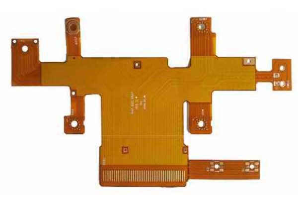
In order to facilitate production, PCB Panel generally needs to design Mark points, V-cut, and Break-up tab.
1、Panel profile
1.1 The profile (clamping edge) of the PCB panel should adopt a closed loop design to ensure that the PCB panel will not be deformed after being fixed on the fixture.
1.2 PCB panel width should be ≤260mm( adopt SIEMENS Surface Mount System) or ≤300mm(adopt FUJI Surface Mount System), if need automatic gluing, then the panel size should be ≤125mm(width) * 180mm(length).
1.3 The shape of the PCB panel is as close as possible to the square. It is recommended to use 2*2, 3*3 …..
2. V-cut
2.1 After V-cut, the remaining thickness should be 1/4~1/3 of board’s thickness, but the least thickness must be ≥0.4mm. The upper limit of the board can be tacken with heavier load, and the lower limit can be taken for the board with lighter load.
2.2 The misalignment of the top and bottom sides of the V-cut should be less than 0.1mm. Due to the limitation of the minimum effective thickness, it is not advisable to use the V-cut method for board with a thickness of less than 1.2 mm.
3. Mark points
3.1 When setting the datum point, usually left a non- solder resist area 1.5 mm larger than around the positioning point.
3.2 The diagonal of PCB board used to assist the optical positioning of the Surface Mount System has at least two asymmetric reference points. The optical positioning point of the panel PCB is generally at the corresponding position of the diagonal of the panel PCB, and the optical positioning point of the each pieces PCB is generally at the corresponding position of the diagonal of the each pieces PCB circuit board.
3.3 For distance ≤0.5mm of QFP (Quad Flat Package) and distance ≤0.8mm of BGA(Ball Grid Array), in order to improve the accuracy of SMT, it is required to set the reference point on both diagonals of the IC.
4. Break-up tab
4.1 There should be no large components or extending components near the connection point between the outer frame of the panel and the inner small boards, between each inner small board also, and the edge of the component and the PCB board should have a space larger than 0.5 mm.
5. Located holes on the board
5.1 Act on the whole board positioning of PCB boards and the reference symbols for fine-distance component positioning, in principle, the QFP with a distance less than 0.65mm should be set at its diagonal position. For the positioning reference symbols each PCB in panel should be used in pairs and set at opposite corners of the positioning elements.
5.2 Large components should have located posts or located holes, such as I/O interface, microphone, battery interface, micro switch, headphone interface, motor and so on.
A good PCB designer should consider the factors of production when making panel design, so as to facilitate processing, improve production efficiency and reduce production cost.