Designing and etching your own Printed Circuit Board prototype is an essential skill for electronics enthusiasts, engineers, and hobbyists. It allows for rapid prototyping, design validation, and small-scale production without relying on external manufacturers. This guide outlines the key steps involved in designing, fabricating, and etching a Printed Circuit Board prototype at home.
Table of Contents
1. What are the tools and steps for PCB design?
The first step in PCB prototyping is designing the circuit layout using PCB design software. Common tools include:

KiCad – Open-source and widely used for professional and hobbyist designs.
Eagle – Offers powerful design tools with an extensive component library.
Altium Designer – Used in professional environments for advanced PCB design.
EasyEDA – Browser-based and user-friendly for quick designs.
Steps in PCB Design:
Schematic Capture – Create the circuit diagram using design software.
Component Placement – Arrange components efficiently to minimize trace lengths.
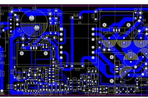
Routing the PCB – Define copper traces connecting components, considering signal integrity and power distribution.
Design Rule Check (DRC) – Validate the design to ensure no errors.
Generate Gerber Files – These files contain the PCB layout data for fabrication.
2. What is the PCB layout for printing?
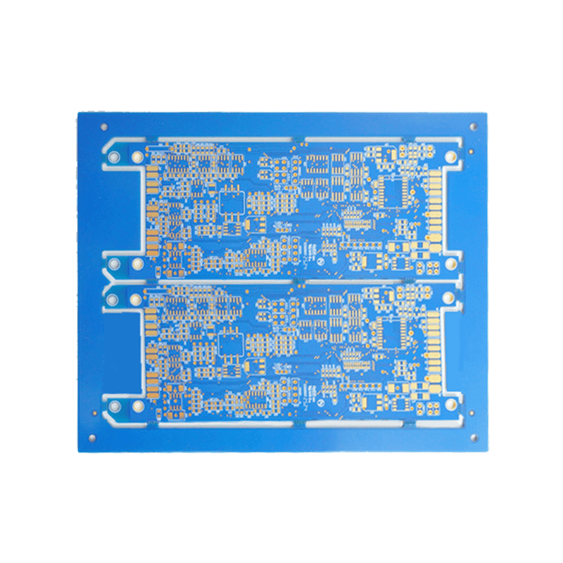
Once the PCB layout is complete, it needs to be transferred onto the copper-clad board.
Methods of PCB Transfer:
Toner Transfer Method – Print the PCB design onto glossy paper using a laser printer and transfer it onto the copper board using heat and pressure.
UV Exposure Method – Use a UV-sensitive board and expose it with a printed transparency film to create the circuit pattern.

3. How to etch PCB?
Etching removes unwanted copper, leaving only the circuit traces.
Steps in Etching:
Prepare Etching Solution – Common etchants include:
Ferric Chloride (FeCl₃) – Effective but stains surfaces.
Ammonium Persulfate – Provides cleaner results but requires precise temperature control.
Hydrochloric Acid + Hydrogen Peroxide – A fast-acting alternative requiring careful handling.
Immerse the PCB – Submerge the board in the etching solution until unprotected copper is removed.
Rinse and Dry – Wash off residual chemicals and dry the board.
4. How to drilling and finishing?
After etching, the PCB requires additional processing to be functional.
Drilling Holes – Use a micro drill to create holes for through-hole components.
Tinning the Traces – Apply solder or tin plating to improve conductivity and prevent oxidation.
Silkscreen and Solder Mask – Optional steps to label components and protect traces.
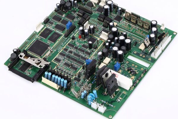
5. How to assemble PCB?
Once the prototype is ready, components are soldered onto the board.
Surface Mount Components (SMD) – Use solder paste and reflow soldering techniques.
Through-Hole Components – Hand solder using a soldering iron.
Conclusion
Designing and etching your own PCB prototype provides flexibility, cost savings, and hands-on experience with PCB fabrication. While home etching has limitations compared to industrial methods, it remains a valuable technique for rapid prototyping and experimental circuits.
Get your exclusive quote immediately: fill out the form or send an email directly.As a professional PCB manufacturer for hobbyist , we will provide you with a quote service within 24 hours. Enjoy free DFM optimization and a 10% discount on SMT patches for your first order!