Table of Contents
1、 Why are there holes on the circuit board?
The holes on the circuit board are mainly based on two major requirements: electrical connection and mechanical structure. Their specific functions are as follows:
1. Electrical connection requirements
-Interlayer conduction: In multi-layer circuit boards, holes can connect wires from different conductive layers to achieve cross layer transmission of signals or power.
-Component pin connection: The pins of plug-in components (such as resistors and capacitors) need to be soldered to the solder pads on the back of the circuit board through holes to form an electrical path.
2. Mechanical structure requirements
-Component fixation: used to fix plug-in components (such as integrated circuits, connectors) to ensure the stability of physical installation.
-Circuit board installation: Fix the circuit board onto the equipment casing or bracket using screws, bolts, etc. through holes.
-Heat dissipation assistance: The mounting holes of some high-power components can assist in heat dissipation or conduct heat through copper layers inside the holes.
3. Process and design requirements
-Via optimization: During dense wiring, vias can shorten the length of the circuit, reduce signal delay or interference.
-Test point reservation: Some holes can be used as probe contact points for circuit testing, which is convenient for debugging.
2、 Definition and Differences of PTH/NPTH/via
1. PTH (Plated Through Hole)
-Definition: The hole wall is covered with a copper layer through electroplating process, making the inner and outer walls of the hole conductive and able to connect different layers of the circuit board.
-Structure and purpose:
-Component mounting holes: The pins of plug-in components pass through PTH holes, and after soldering, electrical connections and mechanical fixation (such as direct insertion resistors and capacitors) are simultaneously achieved.
-Interlayer connection: As a conductive path in multi-layer boards, such as in double-sided boards, the top layer circuit is connected to the bottom layer circuit through PTH holes.
-Features: Copper plated hole walls, with both electrical and mechanical functions, are the most common conductive holes in circuit boards.
2. NPTH (Non Plated Through Hole)
-Definition: The hole wall has no copper plating layer, does not have conductivity, and is only used for mechanical purposes.
-Structure and purpose:
-Mechanical fixation: used for installing non-conductive components such as screws, bolts, brackets, etc. (such as circuit board fixing holes, heat sink mounting holes).
-Installation of non-conductive components: Some components that do not require electrical connections (such as plastic support columns) are fixed through NPTH holes.
-Features: The hole wall has no copper and only serves as physical support, with a lower cost than PTH holes.
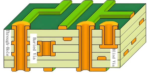
3. Via (via)
-Definition: A hole specifically used for electrical connections between conductive layers of a circuit board, belonging to a special type of PTH, but usually not used for installing components.
-Classification and Usage:
-Through Via: runs through the entire circuit board, connecting the top and bottom layers (or any intermediate layer), such as connecting the upper and lower layers of circuits in a double-sided board.
-Blind Via: It only extends from the surface of the circuit board to the inner layer, without penetrating the entire board, and is used for connecting the surface layer and the inner layer (such as connecting the top layer and the second layer in a four layer board).
-Buried Via: located between the inner layers of a circuit board, not exposed to the surface, used for connecting the inner layers (such as connecting the second and third layers in a four layer board).
-Characteristics: The size is usually smaller than the component mounting hole, and its main function is to shorten the interlayer line distance and optimize the wiring density.
3、 Comparison and application scenarios of the three
| Type | Copper plated or not | Main functions | Typical applications |
| PTH | Yes | Electrical connection+mechanical fixation | Direct insertion component installation, multi-layer board interlayer conductivity |
| NPTH | No | Mechanical fixation | Screw holes, radiator mounting holes |
| Via | is (belongs to PTH) | interlayer electrical connection (non component installation) | interlayer signal transmission in high-density wiring |
4、 Extension: Design considerations for circuit board holes
-Aperture size: It needs to match the pin diameter (PTH) or mounting part size (NPTH) of the component, and the through-hole diameter is usually 0.2mm~1mm.
-Hole spacing: To avoid the risk of decreased circuit board strength or short circuit caused by overly dense holes.
-Process cost: The manufacturing process of blind holes/buried holes is complex and the cost is higher than that of through holes. Therefore, the design needs to be balanced according to the requirements.
By understanding the functions of these holes, one can gain a clearer understanding of the structural design logic of the circuit board, which is fundamental and important knowledge for both hardware development and maintenance debugging.
Get your exclusive quote immediately: fill out the form or send an email directly.As a professional PCB manufacturer for hobbyist , we will provide you with a quote service within 24 hours. Enjoy free DFM optimization and a 10% discount on SMT patches for your first order!