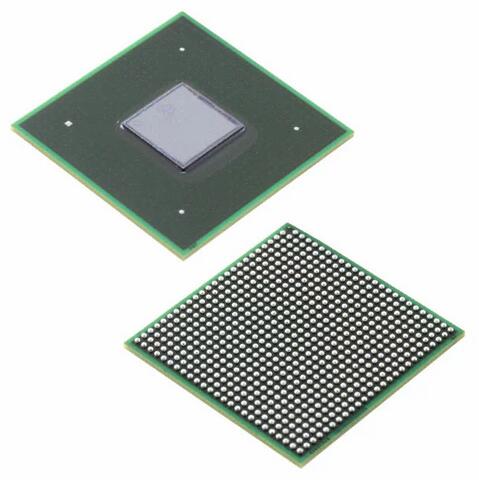
BGA (Ball Grid Array) packaged components are widely used in electronic devices, and their repair process is relatively complex, requiring strict adherence to procedures and attention to details to ensure repair quality and component safety. The following are the main processes and precautions for BGA repair:
Table of Contents
Ⅰ. Main process of BGA repair technology
1. Preparation work
-Equipment and tools:
-Prepare BGA rework table (including heating device, optical alignment system), hot air gun, tweezers, solder suction wire, flux, alcohol, dust-free cloth, etc.
-Confirm that the temperature curve setting of the repair table meets the component specifications (BGA melting points vary depending on the packaging size and material).
-Component and PCB inspection:
-Check if there is any physical damage such as deformation or solder ball detachment on the BGA components to be repaired; Whether the PCB pads are oxidized, damaged, or have residual solder.
2. Dismantle old BGA components
-Heating and dismantling:
-Fix the PCB on the rework table and set the temperature curve according to the BGA size (usually divided into preheating, insulation, reflow, and cooling stages).
-Preheating stage: Slowly raise the temperature to 100-150 ℃, remove moisture from the PCB, and avoid damage to the solder pads due to thermal stress.
-Reflow stage: Heat up to the melting point of the solder ball (Sn63Pb37 about 183 ℃, lead-free solder about 217 ℃), wait for the solder ball to melt, and gently remove the component with tweezers.
-Attention: During the heating process, avoid forcefully prying the components to prevent the solder pads from falling off; Excessive temperature can cause PCB carbonization or component damage.
3. Clean the solder pads and components
-PCB pad processing:
-Use a solder suction wire to remove residual solder from the solder pad, ensuring that the pad is flat and free of oxidation (can be cleaned by applying solder flux and heating).
-If the solder pad oxidizes, it can be lightly sanded with fine sandpaper or wiped with a special cleaning agent, then cleaned with alcohol and blown dry.
-BGA component processing:
-Remove the remaining solder balls and flux at the bottom of the component, and check whether the solder balls and pads are intact; If the solder ball falls off, it needs to be replanted (see step 4).
4. BGA ball placement (if required)
-Ball planting process:
-Fix BGA components and place ball planting steel mesh (with hole diameter matching solder ball diameter) to ensure alignment between the steel mesh and component solder pads.
-Evenly sprinkle solder balls (usually 0.3-0.76mm in diameter, depending on the original packaging) into the steel mesh, and use a scraper to gently remove excess solder balls.
-Apply soldering flux, heat with a hot air gun or repair bench until the solder balls melt, forming a complete solder ball array. After cooling, remove the steel mesh.
-Attention: The size of the solder ball should be consistent with the original packaging. The alignment accuracy of the steel mesh during ball placement directly affects the subsequent welding quality.
5. Alignment and Welding
-Optical alignment:
-Place the processed BGA components in the corresponding positions on the PCB, calibrate them using the optical system of the repair table, and ensure that the solder balls are completely aligned with the solder pads (error ≤ 0.05mm).
-Reflow soldering:
-Set the temperature curve again (slightly lower than the disassembly temperature to avoid overheating of the components), heat until the solder ball melts, and form a solder joint after natural cooling.
6. Inspection and cleaning
-Appearance inspection:
-Visually or with a magnifying glass, observe whether the solder joints are full, without bridging, and whether the components are offset or erected (the “Manhattan” phenomenon).
-Electrical testing:
-Use a multimeter or specialized testing equipment to check the conductivity of solder joints and confirm that they are functioning properly.
-Cleaning residue:
-Use alcohol or specialized cleaning agents to remove solder residue on the surface of PCBs and components, avoiding the risk of corrosion or short circuits.
7. Reliability verification
-If it is a high demand scenario (such as automotive electronics, industrial control), thermal cycling testing (-40 ℃~125 ℃ cycling) or drop testing can be conducted to verify the reliability of solder joints.
Ⅱ. BGA repair precautions
1. Key points of temperature control
-Different solder materials have different melting points (lead-free solder requires higher temperatures), and the temperature curve should be strictly set according to the component specifications to avoid exceeding the temperature resistance limit of the component (usually IC temperature resistance ≤ 260 ℃, duration ≤ 10 seconds).
-The heating rate should not be too fast (recommended ≤ 3 ℃/second) to prevent PCB delamination or internal stress cracking of components.
2. Anti static and cleaning requirements
-Wear anti-static wristbands and gloves throughout the operation, and lay anti-static pads on the workbench to prevent static electricity from penetrating the IC.
-All tools (tweezers, steel mesh, etc.) must be kept clean as residual solder or flux can affect alignment and welding quality.
3. Component and PCB protection
-When dismantling or soldering, avoid direct contact with component pins or PCB pads to prevent contamination or physical damage.
-If the PCB pad is slightly detached, it can be repaired with conductive adhesive or flying wire, but insulation and reliability must be ensured.
4. Alignment accuracy and welding quality
-During optical alignment, it is necessary to calibrate the lens magnification to ensure that the components are perfectly aligned with the solder pads. Minor deviations may cause virtual soldering or short circuits.
-If bridging is found after welding, it can be locally heated and excess solder can be removed with a solder suction wire, but multiple repairs will reduce the lifespan of the PCB (it is recommended to repair the same position ≤ 3 times).
5. Specification for the use of soldering flux
-Choose a soldering flux suitable for BGA soldering (with moderate activity and minimal residue), and do not apply too much to avoid residue affecting insulation or corroding components.
-After welding, it is necessary to thoroughly clean the residual flux, especially the non cleaning flux, as long-term residue may cause electrochemical migration.
6. Requirements for personnel operation skills
-BGA repair requires professional training, and operators need to be familiar with equipment parameter settings, temperature curve optimization, and abnormal handling (such as solder ball detachment and solder pad damage).
-Complex packaging (such as stacked BGA, ultra-thin PCB) requires more careful operation, and if necessary, use an X-ray inspection instrument (AXI) to check the quality of internal solder joints.
Ⅲ.Summary
The core of BGA rework process lies in “precise temperature control, fine operation, and strict inspection”. Errors in each link may lead to rework failure or bury reliability hazards. It is recommended to establish a standardized process based on component specifications and improve the success rate of repairs through regular training and equipment calibration. For high-value or high-density PCBs, professional repair services can be prioritized to reduce risks.
Get your exclusive quote immediately: fill out the form or send an email directly.As a professional PCB manufacturer for hobbyist , we will provide you with a quote service within 24 hours. Enjoy free DFM optimization and a 10% discount on SMT patches for your first order!