>From high-voltage inverters to gigawatt level energy storage systems, the operation of the modern power world increasingly relies on tiny copper wires and silicon wafers embedded in multi-layer circuit boards.
PCB is no longer just a connection carrier for electronic products, it has become a key driver for breakthroughs in power electronics system performance. In the 800V high-voltage platform of new energy vehicles, the new generation of PCB embedded power modules can improve the inverter efficiency to over 99%, achieving a qualitative leap in range. In the field of renewable energy, the output voltage of fuel cell stacks based on PCB technology has jumped to 1050V, eliminating the need for expensive DC/DC boost converters and reducing system costs by 30%. As the power world moves towards higher efficiency and power density, innovative electricity PCB designs are quietly changing the way energy is converted and utilized.
—
Table of Contents
01.Application scenarios of electricity PCB: PCB technology becomes the core support
The power industry has put forward strict requirements for PCBs, including high voltage, high current, strong heat dissipation, and high reliability. The innovative application of PCB is becoming the key to improving system performance and reducing costs.
New Energy Vehicle Electric Drive System: Dual Breakthrough in Efficiency and Density
The popularization of 800V high-voltage platforms has posed unprecedented challenges to inverter PCBs. The high-voltage PCB embedded power module developed by SysPCB directly embeds power chips (such as SiC) into multi-layer PCB boards, significantly shortening the interconnection path.
This integration method reduces switching losses by more than 30%, resulting in an inverter efficiency jump of over 99%. At the same time, the current carrying capacity of the unit semiconductor is increased by 10%, meeting the dual requirements of efficiency and space for high-voltage electric drive systems.

Electric vehicle charging facilities: Thick copper plate supports high-speed charging
The core of high-power DC fast charging piles (such as 350kW+) is to handle high currents of hundreds of amperes. The thick copper plate process developed in collaboration with other manufacturers (with copper foil thickness far exceeding conventional standards) is the key.
The ultra thick copper layer effectively reduces resistance loss, minimizes energy waste and heat generation, and significantly shortens charging time. Its excellent heat dissipation performance ensures that the heat generated by high-power components such as MOSFETs and diodes can be dissipated in a timely manner, ensuring stable operation of the charging station 7×24 hours and extending equipment life.
Renewable Energy Conversion: The Art of Balancing Heat Dissipation and Performance
Solar inverters and wind power converters need to efficiently and reliably convert direct current into alternating current in harsh environments.
Adopting a multi-layer copper layer structure and setting ultra-high thermal conductivity insulation layers between key layers greatly improves the overall heat dissipation capability of the PCB. This design not only reduces the junction temperature of power devices, but also significantly reduces parasitic inductance, improves switching frequency and conversion efficiency, and safeguards the stable output of green energy.
Fuel cell technology: electricity PCB driven voltage revolution
Traditional fuel cell single module output voltage is low (about 0.6V), requiring multi-stage boost conversion. Bramble Energy’s innovative PCBFC ™ The technology utilizes the precision manufacturing and dielectric properties of PCBs to divide film electrodes within a single plane.
This technology increases the output voltage of a single module to 3V. When these electricity PCB modules are stacked, the system output voltage can reach around 1050V, directly matching the power grid or high-voltage load, eliminating the need for expensive DC/DC boost converters, reducing system complexity and cost by 30%, and accelerating the commercial application of hydrogen energy.
—
02 High Power PCB Design Core: Precise Considerations of Materials, Heat Dissipation, and Layout
Design is the cornerstone of electricity PCB performance, and material selection, thermal management, and layout wiring determine the reliability, efficiency, and cost of the system.
Materials Science: Laying the Foundation for Performance
Research by Rogers and other material suppliers suggests that high-power PCBs, especially for RF applications, need to possess four major characteristics: low loss factor (Df), smooth copper foil, high thermal conductivity, and low temperature coefficient of dielectric constant (TCDk).
A smooth copper foil surface can significantly reduce conductor loss at high frequencies, and the insertion loss caused by rough copper foil in thin media is particularly significant. High thermal conductivity laminates (such as ceramic fillers) are the foundation of efficient thermal management.
Thermal Management Technology: Resolving the Challenge of Power Density
Power loss is inevitably converted into heat, especially in RF applications, where the higher the frequency and power, the more severe the heat generation. The Rogers experiment showed that the temperature rise of a microstrip line with 80W power applied at 6.1 GHz was 30 ° C higher than that at 3.6 GHz.
The solution includes: selecting high thermal conductivity substrates (quickly directing heat to the heat sink), optimizing copper foil distribution (increasing heat dissipation area), integrating metal substrates (such as aluminum substrate IMPCB), using thermal vias, and laying thick copper heat dissipation pads with solder mask windows on the outer layer.
Signal and power integrity: the lifeline ensuring stable operation
Signal cross division wiring is a major taboo in high-speed design: in multi-layer PCBs, if high-speed signal lines cross different areas of the reference plane (such as from the GND layer to the power layer or blank area), the return path will be damaged, which will cause serious EMI problems and signal quality degradation (ringing, overshoot).
The design of high and low voltage partitioning is a safety bottom line: on electricity PCBs such as switch mode power supplies and inverters, it is necessary to strictly physically and electrically isolate the high/strong current parts (main power circuit) from the control signal/weak current parts. Clear Creepage&Clearance and reasonable layout can effectively prevent high-voltage noise from “interfering” and causing control circuit misoperation or damage, ensuring system safety and reliability.
—
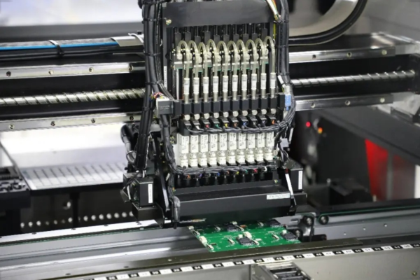
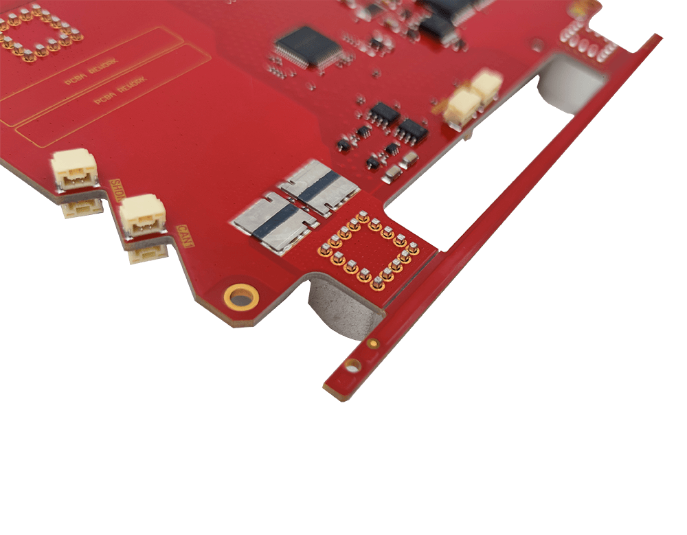
03 Electricity PCB Manufacturing Process: Innovative Practices of Thick Copper, Embedding, and High Reliability
Advanced manufacturing processes are crucial in transforming high-performance designs into reliable products, especially when dealing with extreme requirements in the power sector.
Thick copper plate process: spine carrying high current
The thick copper technology of electricity PCB and other manufacturers is the core support for electric vehicle charging stations, industrial power sources, and power transmission systems. Its copper foil thickness far exceeds conventional standards (up to several ounces or even higher).

The core value of this process lies in low resistance: significantly reducing the electrical energy loss (I ² R Loss) during high current transmission. Meanwhile, the thick copper layer itself is also a good thermal conductor, and its excellent heat dissipation performance, in conjunction with external heat dissipation solutions, ensures the long-term stable operation and lifespan of high-power equipment.
Embedded Packaging (EDP): A Leap in Integration and Performance
The PCB embedded power chip solution we are promoting is an important trend in power electronic packaging. Directly embed the die into the multi-layer structure of the electricity PCB.
This structure significantly reduces interconnect thermal resistance, improves heat dissipation capacity, and increases unit current carrying capacity by about 40% (meaning fewer chips can be used at the same current, reducing costs). At the same time, the extremely short interconnection reduces the on resistance and parasitic inductance, reduces switching losses and EMI, and improves system efficiency and reliability.
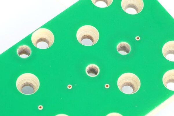
Micro pores and fine circuits: the cornerstone of high-density interconnect (HDI)
Modern power control systems, such as motor controllers and BMS control boards, are becoming increasingly complex and miniaturized, relying on HDI technology. This includes laser micropores (with diameters up to micrometers), multi-layer stacking, and fine lines/spacing.
Micro porous technology enables denser interlayer interconnections, and fine lines meet the requirements of complex wiring and higher signal density, providing a physical foundation for the miniaturization, multifunctional integration, and performance improvement of power electronic devices.
High reliability special process: guarantee against harsh environments
Pad Optimization: Thickening and optimizing the copper layer around the borehole (especially high current holes) to enhance the connection strength between the borehole wall and the inner/outer circuit, effectively preventing borehole wall fracture (Barrel Crack) or delamination under thermal cycling and mechanical vibration.
Other key processes include strict process control (to avoid ion contamination), selection of high-performance substrates (high TG, CAF resistance), enhanced surface treatment (such as thick gold plating for high-voltage connectors), etc., to ensure the long-term reliability of PCBs in typical harsh environments of power equipment such as high temperature, high humidity, and strong vibration.
—
04 Future Trends: PCB Breaks Boundaries, Empowers Green Energy and Intelligent Power
Technological progress and market demand are driving the development of power PCBs towards higher performance, wider applications, and more sustainable directions.
AI and data center: driving the surge in demand for high-end PCBs
Some institutions predict that by 2027, the global PCB industry’s output value will reach 98.388 billion US dollars.
AI servers and data centers are the core growth engines, with extremely strict requirements for PCBs: ultra-high density cabling (supporting more I/O and memory), ultra high speed signal transmission (112Gbps+), and extremely low loss and noise.
Data shows that the global server PCB market size is expected to reach approximately 8.2 billion US dollars in 2023, and is projected to soar to 13.8 billion US dollars by 2028, with a compound annual growth rate of up to 11%, making it the strongest growing sector among all PCB application areas. High multilayer boards, high-speed materials (such as M7/Low Dk Df), advanced HDI, and backplate technology are the focus of competition.
High voltage transformation of new energy vehicles: continuous iteration of PCB technology
The accelerated popularization of 800V/1000V or even higher voltage platforms in electric vehicles has raised higher requirements for the insulation performance, voltage resistance level, and thermal management of PCBs. The peak voltage of SysPCB’s high-voltage PCB embedded power module can reach up to 930V, demonstrating its technological potential.
The output value of automotive PCBs is expected to increase to 14.5 billion US dollars by 2026, accounting for 15% of the overall PCB output value, with a compound annual growth rate of about 12% from 2022 to 2026. The basic requirements for automotive grade high reliability, high temperature and humidity resistance, and adaptability to complex electromagnetic environments are embedded technology, thick copper, and high thermal conductivity materials, which will be more widely used.
Green hydrogen production: PCB electrolytic cell opens up a new track
PCB technology is being applied across borders to the key equipment for green hydrogen production – electrolytic cells. The Printed Circuit Board Electrolytic Cell (PCEC) developed by Bramble Energy utilizes mature PCB manufacturing facilities and supply chains to achieve low-cost, rapid, and large-scale production.
Its modular design greatly simplifies the structure of the electrolytic cell, reduces the complex components of traditional electrolytic cells such as end plates, seals, and manifolds, significantly reduces manufacturing costs and potential failure points, and provides a new technological path for large-scale green hydrogen production.
System level packaging (SiP) and integration: “inverter brick” leads a new form
The key to improving power density and system efficiency lies in integration. The design of “inverter bricks” that integrate power modules, DC support bus capacitors, gate drive boards, and even control units has become a new trend.
The newly developed 800V silicon carbide embedded power module inverter brick is a typical representative. This highly integrated approach reduces the complexity of wiring harnesses and connectors within the system, lowers parasitic inductance and resistance, improves system efficiency, power density, and reliability, while simplifying overall assembly.
—
By 2030, the global market penetration rate of high-voltage platforms for new energy vehicles will exceed 65%, and each 800V electric vehicle will require 40% more PCB area than traditional models.
The path from laboratory to industrialization is shortening. Enterprises that have mastered high-power PCB design, material application, and advanced manufacturing process capabilities are actively laying out their energy landscape for the next decade. When your product needs to carry higher voltage, smarter control, and more harsh environments, the precision copper wire network hidden deep in the insulation layer – their design and manufacturing level – will directly determine the performance height and application boundaries of power electronic systems.
—
The application prospects of PCB in the field of power are broad and clear. The automotive PCB market is expected to reach 14.5 billion US dollars by 2026, with a compound annual growth rate of up to 12%. The global server PCB market is expected to grow to $13.8 billion by 2028, with a compound annual growth rate of 11%. The emerging PCB electrolytic cell technology is expected to significantly reduce the cost of green hydrogen. The combination of innovative processes and cutting-edge applications is driving PCB technology to become the core cornerstone for building future efficient, intelligent, and green energy systems.