In the wave of high-performance and differentiation in electronic devices, standard PCBs are no longer able to meet the requirements of complex scenarios.custom PCBs are becoming a core choice in fields such as industrial control, medical equipment, automotive electronics, and communication base stations by accurately matching electrical performance, mechanical structure, and special environmental requirements. Through multi-layer stacking design, special material adaptation, and high-density interconnect technology, customized solutions can improve equipment stability by more than 30% and shorten product launch cycles.
Table of Contents
01 custom PCB Full Process Analysis: Key Steps from Requirement to Delivery
Deep integration of requirements and custom PCB design collaboration
-Customization begins with a precise understanding of the application scenario: jointly confirming the circuit function objectives, working environment (temperature/vibration/corrosion resistance), signal type (high frequency/high current), and space limitations with the customer, forming a technical specification document.

-Design simulation synchronization optimization: Use SI/PI (signal/power integrity) simulation tools to predict interference risks, optimize stacked structures and wiring strategies, and avoid rework in the later stage.
Materials Science: The Foundation of Performance
-The substrate determines the upper limit of the system:
-High frequency scenario: Choose ceramic filled PTFE (Df<0.002) or Rogers RO4000 series (Dk=3.0-3.58) to ensure low loss signal transmission.
-High heat dissipation requirements: Aluminum or ceramic substrate (thermal conductivity>2W/mK), suitable for LED lighting and power modules.
-Extreme environment: Polyimide (PI) flexible material or high Tg FR-4 (Tg>170 ℃), to cope with vibration in automotive engine compartments or aerospace.
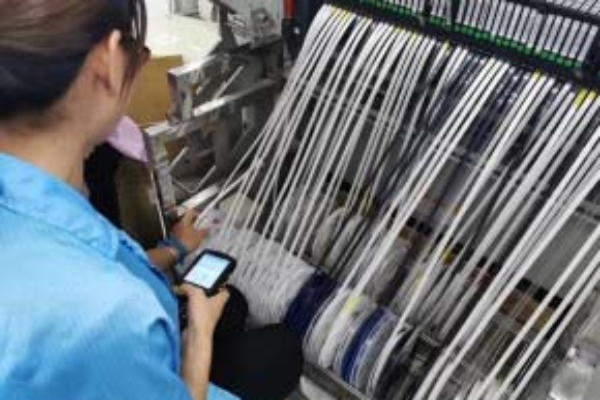
Precision manufacturing and rigorous quality inspection
-The core process chain is fully controllable throughout:
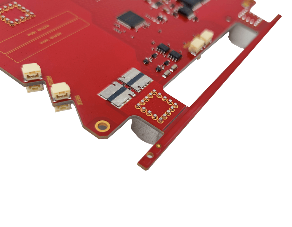
1. Laser drilling: achieve 0.1mm micro blind holes, support HDI interconnection of any layer;
2. Differentiated etching: Thick copper plates (2-20oz) adopt side etching compensation technology to ensure the accuracy of high current circuits;
3. Surface treatment: ENEPIG combines solder joint strength (>45MPa) and aluminum wire bonding ability, suitable for BGA packaging.
-Zero tolerance testing: AOI automatic optical inspection+flying needle testing to troubleshoot open/short circuits, X-ray fluoroscopy of inner buried holes and solder joints, ensuring a yield rate of>99.95%.
02 Irreplaceable Customization Advantage: Why do leading companies choose custom PCBs?
The ultimate balance between space and performance
-High density integration releases design freedom:

By using blind buried holes and disk hole technology, the component layout density is increased by 40%, the high-speed signal path is shortened, and parasitic inductance is reduced – smartphone motherboards achieve billions of transistor interconnections within 10 layers.
-Breakthrough in heat dissipation and current carrying capacity:
Thick copper design (10oz) supports 100A+continuous current, and the copper layer is directly welded with TO-220 heat sink, helping the efficiency of photovoltaic inverters exceed 98%.
Agile Response and Risk Control
-Rapid prototyping accelerates research and development: High end factories support 24-hour expedited prototyping, delivering small batches within 3-5 days, shortening product validation cycles by 50%.
-Cost reduction and efficiency improvement in panel production: Multiple designs are combined for production, sharing the cost of steel mesh and equipment debugging, and reducing the price of small batch orders by 30%.
Reliability Design for the Future
-Enhanced environmental adaptability:
-Military grade PCB has passed the 1000 cycle test at -40 ℃~125 ℃;
-ENEPIG coating is resistant to sulfide corrosion, ensuring a 10-year lifespan for offshore communication equipment.
-Compliance certification guarantee: ISO9001, IATF16949 (automotive regulations), UL certification build the cornerstone of global market access.
03 Overcoming Industry Pain Points: Innovative Application of High end Customization Technology
High power electronic customization solution
–New energy vehicle 800V platform:
Thick copper+ceramic substrate mixed pressure technology to solve the thermal failure problem of IGBT modules; Embedded power chips (such as SiC) reduce parasitic inductance and improve inverter efficiency to 99%.
-5G base station millimeter wave antenna:
The high-frequency hybrid board (RO4350B+FR-4) achieves 64 unit/board integration, with insertion loss<0.5dB, meeting the transmission requirements of the 28GHz frequency band.
Core technology of miniaturized equipment
-Disk hole (VIPPO):
Directly drill holes and fill copper in the solder pads to eliminate the bottleneck of BGA area winding – the size of the smartwatch motherboard is reduced to 25mm × 30mm.
-Soft hard combination board:
The hinge area of the foldable screen mobile phone adopts a 3D structure PCB, with a bending life of over 200000 times.
04 Cost optimization strategy: Customization does not equal high cost
| Cost drivers | Cost reduction strategies | Effectiveness |
| Special materials (such as Rogers) | High frequency local mixed pressure+domestic ceramic substrate | Material cost reduced by 40% |
| Number of high layers (>12L) | Blind buried holes replace through holes+optimized stacking | Reduce 2-4 layers, cost reduction of 15-25% |
| Small batch production | Panel design+shared panels | Unit cost reduced by 30% |
The Future of custom PCBs: Green Manufacturing and Intelligent Factories
-Breakthrough in Sustainable Materials:
Halogen Free substrate and gold deposition process wastewater recovery rate>95%, in compliance with the EU RoHS 3.0 standard.
-AI driven intelligent manufacturing:
The deep learning visual inspection system recognizes 25 μ m defects, reduces equipment downtime through predictive maintenance, and increases production capacity utilization to 90%.
When the global high-frequency PCB market is growing at a compound annual growth rate of 11% towards a scale of billions, customization has changed from an “optional” to a “mandatory” option.
>In the SysPCB project, by customizing an 18 layer thick copper HDI board, the volume of the motor controller was reduced by 40%, the thermal resistance was reduced by 40%, and the mass production yield exceeded 99.2% – this is not only a technological victory, but also a value proof for accurately defining requirements.
We provide not only circuit boards, but also full stack solutions from requirement analysis to mass production delivery. Our own factory ensures controllable processes, and our 7 * 24 sampling team is always responsive, allowing your innovation to take place without waiting.