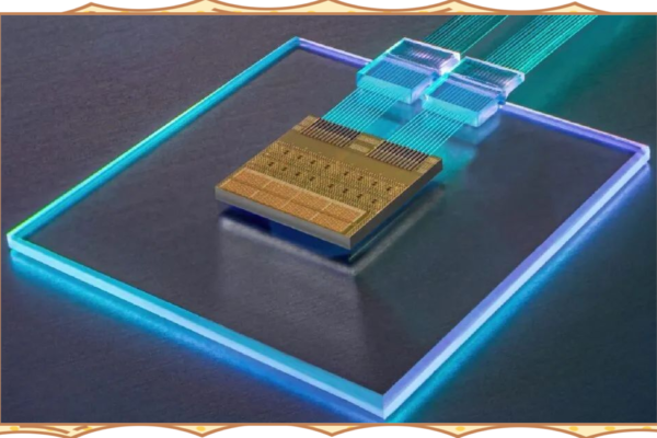
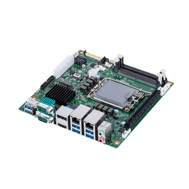
With the popularization of 5G communication, AI chips, and new energy equipment, the power density of electronic devices is growing exponentially, and PCB heat dissipation design is facing unprecedented challenges. As an SMT and PCB manufacturing enterprise, we deeply analyze industry pain points and help customers overcome thermal management bottlenecks.
Table of Contents
Challenge 1: Imbalance between power density surge and heat dissipation efficiency
According to market research, the global PCB heat sink market has reached $1.5 billion in 2024 and is expected to exceed $2.8 billion by 2030. However, as the chip process enters nodes below 3nm, the power consumption per unit area sharply increases. For example, Nvidia’s new generation AI GPU has a power consumption of up to 1000W, while traditional air cooling solutions are approaching their heat dissipation limits.
Core issue:
-Sudden increase in heat flux density: Advanced architectures such as nanosheet transistors (CFETs) have increased chip power density by 12% -15% compared to the previous generation, with local temperatures rising up to 9 ° C.
-Risk of thermal runaway: High temperature can cause an increase in leakage current, forming a “temperature power consumption” positive feedback loop, threatening equipment stability.
Technological breakthrough direction:
-Microfluidic heat dissipation: Etching micro level cooling channels inside the chip, directly contacting the heat source to achieve efficient heat dissipation.
-Back Power Supply Network (BSPDN): reduces heat generation by lowering resistance, but needs to address the issue of decreased lateral heat dissipation caused by thinning of the silicon substrate.
Challenge 2: The contradiction between miniaturization and heat dissipation space
The requirements for PCB size in consumer electronics and medical devices are becoming increasingly stringent, and heat dissipation design needs to balance performance and reliability within a limited space.
Typical case:
-Folding screen phone: The PCB thickness in the pivot area is compressed to 0.3mm, making it difficult to embed traditional heat sinks and relying on flexible aluminum substrates and laser micro hole technology.
-Satellite communication module: The space vacuum environment cannot dissipate heat through convection. The stepped “copper coin” structure developed by OKI improves heat dissipation performance by 55 times by increasing the contact area.
Innovative solution:
-Embedded heat dissipation structure: such as copper coins, T-shaped/C-type thermal blocks, directly embedded under high heating elements.
-3D Stacked Heat Dissipation: Utilizing multi-layer PCBs with embedded heat dissipation layers, vertical heat conduction is achieved through metalized vias.
Challenge 3: Breakthrough of Materials and Craftsmanship Limits
Traditional heat dissipation materials (such as FR4) have a thermal conductivity of only 0.3W/m · K, making it difficult to cope with high-power scenarios.
Material bottleneck:
-Cost performance trade-off: Copper substrate has a thermal conductivity of 400W/m · K, but its cost is three times that of aluminum substrate.
-High temperature stability: The temperature resistance of polyimide substrate is insufficient, and a high heat-resistant copper-clad laminate with TG ≥ 170 ℃ needs to be developed.
Technological innovation:
-High precision manufacturing: Laser drilling technology achieves 50 μ m micro hole processing, improving the distribution density of heat dissipation holes.
-Composite cooling design: Combining heat pipes, heat sinks, and liquid cooling systems, such as the immersion cooling scheme used in data centers.
Challenge 4: Reliability assurance in extreme environments
The fields of automotive electronics, aerospace, etc. require PCBs to operate stably under extreme conditions such as temperature differences of -55 ℃~260 ℃ and high-frequency vibrations.
Industry pain points:
-Thermal stress failure: Mismatched coefficient of expansion of materials leads to cracking of solder joints, requiring the use of low CTE ceramic substrates (such as aluminum nitride).
-Vacuum heat dissipation obstacle: Space equipment relies on thermal radiation for heat dissipation, and surface blackness coating and thermal radiation area need to be optimized.
Conclusion: Collaborative innovation breaks through the heat dissipation dilemma
PCB heat dissipation has shifted from single technology research to system level collaborative design. In the future, enterprises need to focus on materials science (such as graphene heat dissipation film), process innovation (such as 3D printed heat sinks), and intelligent management (AI temperature control algorithm) to meet the demands of higher power density and more demanding environments.
As a technology service provider deeply involved in electronic manufacturing, we provide end-to-end solutions from selecting high thermal conductivity materials to optimizing heat dissipation structures, helping customers overcome heat dissipation challenges. [Click to get customized heat dissipation design solution]