>When a circuit board moves from a design to an intelligent terminal, these professional terms form the common language of the manufacturing process
Understanding core terminology is the cornerstone of efficient collaboration in the precision chain of electronic manufacturing industry. As a PCB company, we are well aware that our customers are often troubled by professional abbreviations such as BOM, DIP, SMT, SMD, etc. This article will take the production process as the context to deeply analyze the technical connotations and practical value of the four key concepts.
Table of Contents
1、 BOM (Bill of Materials): DNA profile of electronic manufacturing
Definition: Bill of Materials, a structured data file that records all materials required for a product, is the core hub connecting design and manufacturing.
Technical analysis:
Typical BOM hierarchical structure
| Level | Content | Example |
| L1 | Finished product model | Intelligent controller V3.0 |
| L2 | PCBA module | Main control board – Layer 6 HDI |
| L3 | Components/Raw Materials | IC: STM32H750VBT6 |
| L4 | Accessories | Solder Paste: SAC305 |
Practical value:
-Cost control: Accurately calculate the cost of single board materials (a certain industrial controller BOM contains 187 items, with a cost error of<0.5%)
-Supply Chain Management: Identify long lead time materials (such as automotive grade MCUs that require preparation 26 weeks in advance)
-Version tracing: Record every ECN change (to avoid batch accidents caused by mixing old and new materials)
Industry pain point: A medical device suffered a loss of 370000 yuan due to the BOM not indicating “lead-free process”, resulting in the rework of 2000 boards.
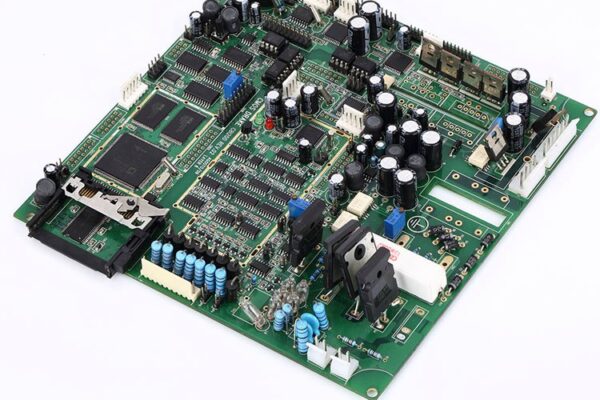
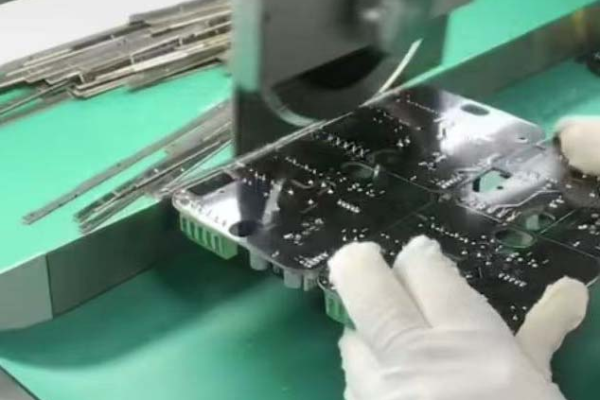
2、 DIP (Dual In Line Package): The Survival Rule of Traditional Devices
Definition: Dual In line Package, a component packaging form in which pins are led out from both sides of the package and require through-hole soldering.
Technological evolution:
| Parameters | Traditional DIP | Modern Improved Type |
| Pin spacing | 2.54mm | 1.78mm (HDIP) |
| Pin count | 4-64 | Maximum 128 (SDIP) |
| Welding method | Wave soldering | Selective wave soldering |
Irreplaceable scenarios:
-High power devices: Relay/transformer pins carry current>10A (SMD devices typically<5A)
-Mechanical strength requirement: Industrial connector insertion and extraction force>50N (DIP through-hole soldering resistance is 3 times that of SMD)
-Extreme environment: Under thermal cycling from -55 ℃ to 125 ℃, the failure rate of DIP solder joints in military equipment is only 1/5 of that of SMD

Production warning: The layout of DIP devices should follow the 3mm spacing rule to avoid virtual soldering caused by shadow effects during wave soldering.
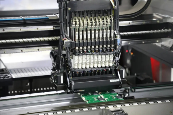
3、 SMT (Surface Mount Technology): The Efficiency Revolution of Modern Electronics
Definition: Surface Mount Technology is a process system that directly mounts components onto the surface of PCB pads.
Full process technical diagram:
| graph LR A [Solder Paste Printing] –>B [SPI Testing] B –>C [High speed SMT] C –>D [Reflow soldering] D –>E [AOI detection] |
Core parameter breakthrough:
-Precision evolution: from early ± 100 μ m to ± 25 μ m (equivalent to 1/3 of a hair strand)
-Miniaturization limit: capable of handling 01005 packaged components (0.4 × 0.2mm)
-Temperature control: Temperature difference of nitrogen reflow soldering in the ten temperature zone is ≤± 1.5 ℃
Benefit comparison (with traditional DIP production line):
| Indicators | SMT production line | DIP production line |
| Production efficiency | 150000 points/hour | 20000 points/hour |
| Component density | 25 pieces/cm ² | 8 pieces/cm ² |
| Solder joint defect rate | <200ppm | 800-1500ppm |
—
4、 SMD (Surface Mount Device): The Cell Unit of the Miniaturization Era
Definition: Surface Mount Device, a pinless packaged component designed specifically for SMT processes.
Full parsing of encapsulation types:
| Packaging family | Typical models | Application scenarios | Welding challenges |
| Chip component | 0201 resistor | Mobile RF circuit | Monument phenomenon |
| QFP | TQFP-100 | Industrial Control MCU | Pin Coplanarity ≤ 0.1mm |
| BGA | 0.4mm pitch | GPU chip | Hole rate control |
| QFN | Heat dissipation pad type | Power management IC | Tin climbing height monitoring |
The Golden Rule of Selection:
1. Thermal matching principle: The CTE of the component should have a difference of less than 5ppm/℃ from the PCB substrate (such as ceramic capacitors matched with high-frequency boards)
2. Moisture sensitivity level: Welding of MSL3 or above devices must be completed within 72 hours after unpacking
3. Pad design specification: BGA pad diameter=ball diameter x 0.8, to prevent bridging
Blood and tears lesson: A certain enterprise did not bake according to MSL level, resulting in a “popcorn effect” during BGA chip reflow soldering, with a batch scrap rate of 22%.
5、 Terminology collaboration: gear meshing in the manufacturing process
Typical PCBA production chain:
| 1. Design output → [BOM file] → Material procurement 2. Incoming inspection → [SMD components] → SMT production line 3. Hybrid process → [DIP device] → Selective wave soldering 4. Functional testing → BOM version verification → Finished product shipment |
Key collaborative nodes:
-BOM and SMT: Component part numbers must match the Gerber file 100% (1 character error can cause the entire board to be mounted incorrectly)
-SMD and DIP: During layout, SMD should be at least 3mm away from DIP sockets to avoid soldering interference
-Process selection: High frequency modules prioritize SMT (reducing pin inductance), while power modules retain DIP (enhancing mechanical strength)
Technological Frontier: The Manufacturing Revolution Behind Terminology
Micro assembly evolution:
-01005 component mounting accuracy reaches ± 15 μ m (equivalent to the diameter of red blood cells)
-3D solder paste printing technology achieves 0.03mm ³ volume control
-Femtosecond laser welding reduces the heat affected zone to 10 μ m
Intelligent control:
-BOM cloud collaboration platform realizes real-time supply chain warning
-AOI+AI visual system defect recognition rate increased to 99.2%
-Digital twin technology rehearses welding process, reducing trial production cycle by 70%
When a mobile phone motherboard carries 3000 SMD components and is precisely mounted at a speed of 18 per second, and the DIP solder joints on the aerospace controller remain intact after thousands of cycles at -55 ℃~125 ℃ – these underlying passwords that create miracles are the precise control of BOM, DIP, SMT, and SMD.
Mastering these terms is not only a communication tool, but also a key to understanding the precision, complexity, and synergy of modern electronic manufacturing. Under the dual challenges of miniaturization and high reliability, we inject practical value into each term with a process control accuracy of ± 10 μ m and a million level BOM database – because true professionalism begins with an ultimate understanding of fundamental concepts.