>From the wiring substrate of the vacuum tube era to the intelligent carrier of the 5G era, electronic interconnection technology has undergone a genetic leap from PWB to PCB.
In the terminology system of electronic manufacturing industry, PWB (Printed Wiring Board) and PCB (Printed Circuit Board) are often mixed, which actually hides the technical code of industry evolution. As a technical team with 20 years of experience in the field of electronic interconnection, this article will deeply analyze the differences between the two and reveal the core breakthroughs of modern PCB technology.
—
Table of Contents
1、 Terminology traceability: from wiring carriers to functional circuits
▶ PWB: The Physical Essence of Wiring Boards
-Historical positioning: Born in the 1940s, specifically referring to basic boards that only achieve electrical interconnection, like the “road network” of electronic components
-Typical features:
-Mainly single/double panels, with no functional connections between layers
-No impedance control requirement, line width tolerance ± 20%
-Surface only treated with tin spray or bare copper

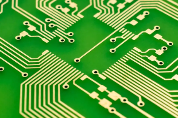
▶ PCB: The Engineering Carrier of Circuit Systems
-Technological leap: After the 1970s, with the rise of integrated circuits, it was upgraded to a system platform that carries circuit functions
-Core Evolution:
-Multilayer structure (4-60 layers) for high-density interconnection
-Integrated impedance control, electromagnetic shielding and other electrical performance design
-Diversified surface treatment processes (such as immersion gold, immersion silver, OSP, etc.)
Industry consensus: In modern standards, PCB has become a super term that covers PWB. The IPC-6012 standard clearly defines multi-layer boards HDI、 Rigid flex boards and other components are included in the PCB category.
—
2、 The watershed of material systems
Limitations of PWB Era
| Material type | Defect | Typical failure case |
| Paper based phenolic resin | Temperature resistance<130 ℃, undefined Tg value | Welding foaming rate>35% |
| Epoxy fiberglass cloth base | dielectric constant fluctuation ± 0.8 | signal distortion rate up to 12% |
The technological revolution of PCB materials
-High frequency material: Rogers RO4000 series (Dk=3.38 ± 0.05), ensuring the integrity of 77GHz millimeter wave radar signals
-High thermal conductivity substrate: Beige 92ML aluminum substrate (thermal conductivity of 2.5W/m · K), solving the bottleneck of automotive electronic heat dissipation
-Flexible material: DuPont Pyralux AP (resistant to bending>200000 times), supporting the circuit in the hinge area of foldable screen phones
—
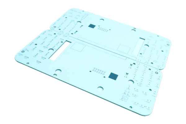
3、 Comparison of structural complexity
1. Evolution of Inter Layer Interconnection Technology
-PWB era: only through-hole connection, aperture>0.8mm, density<5 holes/cm ²
-PCB breakthrough:
-Laser micro hole: 50 μ m blind hole for arbitrary layer interconnection (such as iPhone motherboard 20 layer HDI)
-Embedded components: resistors and capacitors embedded in the board, reducing surface solder joints by 30%
2. Evolution history of line accuracy
| Parameters | PWB Standard (1980s) | Modern PCB Standard | Technological Enhancement Efficiency |
| Minimum line width | 0.3mm | 0.025mm | Increased wiring density by 12 times |
| Aperture tolerance | ± 0.10mm | ± 0.025mm | High frequency connector yield>99% |
| Interlayer alignment accuracy | ± 0.15mm | ± 0.025mm | 20 layer board yield increased by 40% |
—
4、 The essential differences in functional attributes
PWB: Single Interconnected Carrier
-Core mission: Provide electrical connection channels for components
-Design Thinking: Addressing Connectivity Issues
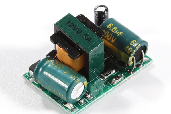
PCB: Systematic Solution
-Signal integrity engine:
-100 Ω differential impedance control (tolerance ± 7%)
-Serpentine routing length matching error ≤ 5ml
-Thermal management platform:
-Heat dissipation through-hole array (aperture 0.2mm/spacing 0.4mm)
-Localized 2oz thick copper design reduces thermal resistance
-Electromagnetic compatibility fortress:
-Shielded cavity design (attenuation>60dB)
-Hybrid grounding technology eliminates ground bounce noise
—
5、 Intergenerational leap in manufacturing technology
Traditional PWB process bottleneck
-Graphic transfer: Wet film exposure, line width deviation>20%
-Hole metallization: chemical deposition copper adhesion<1.0N/mm
-Solder mask process: screen printing thickness deviation ± 15 μ m
Breakthrough in modern PCB core technology
-Laser direct imaging (LDI):
8 μ m alignment accuracy, supporting 3mil line width (deep south circuit scheme)
-Pulse electroplating hole filling:
Blind hole copper filling depression<5 μ m (New Optoelectronics Technology)
-Nano coating solder mask:
Shrinkage rate of plug hole ink<0.3% (solar ink TF-1000)
Yield comparison: Automotive electronic PCBs have reduced their micro short defect rate from 500ppm in the PWB era to<50ppm through process upgrades
—
6、 Selection decision tree: PWB or PCB?
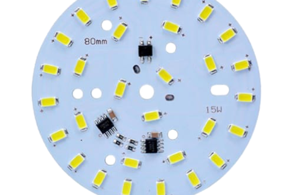
▶ Choose the three major scenarios for PWB
1. Pure mechanical support components such as consumer electronics casing and lining
2. Low power LED lighting board (current<1A)
3. Educational electronic kit (without high-frequency signal)
▶ Fields where PCB must be used
| Application scenarios | Technical requirements | Recommended processes |
| 5G base station | 77GHz millimeter wave transmission | ultra-low loss material+hybrid stack |
| Autonomous driving | 12 layer board temperature resistance of 150 ℃ | High Tg material+filled copper holes |
| Medical endoscope | Flexible circuit resistant to thousands of bending cycles | 2-layer rigid flex bonding board |
—
Conclusion: Reshaping Value Boundaries in Evolution
The transition of terminology from PWB to PCB is essentially a paradigm revolution of electronic interconnect technology from “connecting carriers” to “functional systems”. When a server motherboard carries trillions of calculations per second, when a pacemaker circuit works in the body for ten years – modern PCBs have surpassed the scope of physical substrates and evolved into a micro ecosystem that integrates materials science, electromagnetics, and thermodynamics.
>Intel senior academician Roger Dumas pointed out:
>The ultimate mission of PCB is to enable electronics to dance accurately between every inch. ”
As a manufacturing enterprise certified by both IATF16949 and ISO13485, we provide a full range of solutions from high-density PWBs to cutting-edge PCBs. Whether it is the thick copper design of industrial control boards or the mixed layer stacking of satellite communication boards, they are based on the IPC Level 3 standard – because more important than circuit conductivity is a reliable commitment spanning ten years.