>Behind each high-definition image, there is a precision circuit board that completes the conversion and transmission of optoelectronic signals in milliseconds.
As the core carrier of imaging equipment, camera PCB is not only the physical support platform for electronic components, but also the key hub for realizing photoelectric signal conversion, data processing, and image generation. With the rapid development of smartphones, security monitoring, and industrial vision, camera PCB design has been upgraded from basic interconnection to a cutting-edge technology field that integrates high-frequency transmission, miniaturization, and anti-interference. This article will deeply analyze the full chain technology architecture and manufacturing system of camera PCB.
—
Table of Contents
1、 What is a camera PCB?
Camera PCB is a printed circuit board designed specifically for imaging devices, responsible for the electrical interconnection and mechanical support of image sensors, processors, and optical components. Its core features are manifested as:
-High density wiring: It is necessary to integrate thousands of signal nodes in a limited space. For example, the PCB of a smartphone camera module often adopts an HDI design with more than 8 layers, and the line width/spacing is ≤ 3mil (0.075mm);
-High frequency anti-interference: To ensure the transmission of GHz level image data, strict impedance control (tolerance ± 7%) is required, and a shielding cover is used to isolate electromagnetic noise;
-Miniature structure: The PCB area of mobile phone cameras can be as small as 10 × 10mm, and rigid flex boards are commonly used to adapt to folding space;
-Thermal management design: The power consumption of the image processor can reach 3-5W, and it needs to be equipped with copper protrusions or heat dissipation through holes to dissipate heat.
According to the China Academy of Commerce Industry Research, the size of China’s PCB market is expected to reach 346.9 billion yuan by 2024, with camera related PCBs growing by over 15% in the consumer electronics and automotive sectors.
—
2、 Key components of camera PCB module
1. Camera PCB Image sensor interface
-Pad array: Micro pitch BGA pads (0.3mm pitch) are directly connected to CMOS sensors and require ENIG surface treatment to prevent oxidation;
-Ladder structure: The patented PCB ladder design enhances the bonding strength of the housing and reduces imaging blur caused by lens offset.
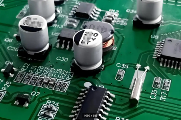
2. Clock and signal conditioning unit
-High stability crystal oscillator: such as Epson FA-128 48MHz crystal oscillator (± 15ppm accuracy), ensuring image acquisition synchronization, with an annual aging rate of only ± 1ppm;
-High speed transmission line: The impedance of differential pair routing is controlled at 100 Ω± 10%, and the length matching error is ≤ 5ml.
3. Power management network
-Separate analog/digital ground planes in multi-layer boards and use star topology power supply to reduce sensor noise;
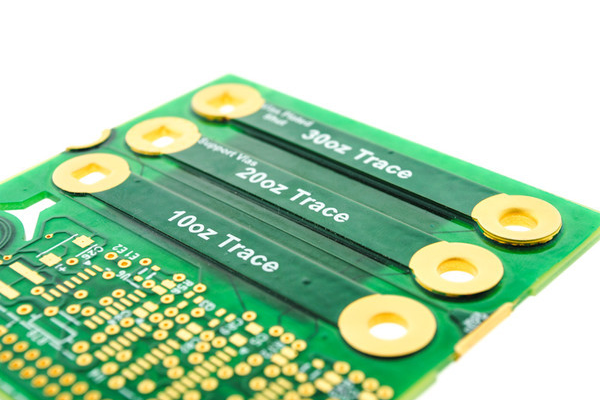
-The high current path uses 2oz thick copper to reduce the impact of voltage drop on the dynamic range.
—
3、 The Four Core Functions of Camera PCB
1. Optoelectronic conversion center
Convert the analog signal of the CMOS sensor into a digital signal and transmit it to the processor through a 12 channel MIPI interface, with a speed of up to 10Gbps.
2. Precise control of optical components
Drive autofocus (VCM motor) and optical stabilization (OIS coil), with a controlled current accuracy of ± 2mA.
3. Thermal stability guarantee
-Aluminum substrate or copper paste plug hole design reduces the hot spot temperature by 15 ℃;
-The rigid joint plate absorbs equipment vibration and impact, improving the reliability of the car camera.
4. EMI/EMC protection system
-0201 encapsulated magnetic bead array filters out GHz noise;
-The edge grounding shield blocks radiation leakage.
—
4、 Core specifications of camera PCB
| Parameter Category | Consumer Standard | Industrial Standard | Key Impact |
| Layer number | 6-8 layers HDI | 10 layers+arbitrary layer interconnection | Wiring density and signal integrity |
| Line width/spacing | 3/3mil | 2/2mil | Micro pad lead out capability |
| Surface Treatment | ENIG (Gold Thickness 0.05 μ m) | Electroplated Hard Gold (Gold Thickness 0.5 μ m) | Solder Joint Reliability |
| Maximum aperture tolerance | ± 0.05mm | ± 0.02mm | Lens module alignment accuracy |
| Working temperature | -20 ℃~85 ℃ | -40 ℃~125 ℃ | Automotive/outdoor applicability |
—
5、 Analysis of high-end production technology
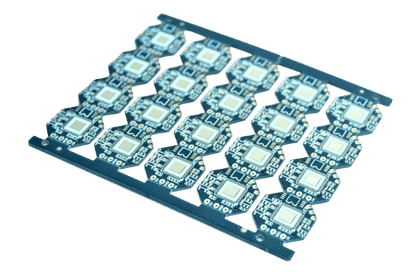
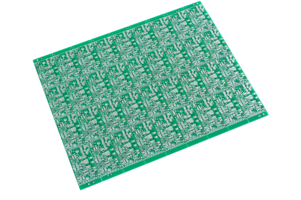
1. High density interconnect (HDI) process
-Laser micro hole: CO ₂ laser drilling 50 μ m blind hole, connecting image sensor and inner layer wiring;
-Stacked hole structure: The second-order HDI adopts a staggered stacked hole design to avoid copper fracture in the holes (such as the Shennan circuit scheme).
2. Precise impedance control
-Mixed layer stacking: Rogers 4350B (Dk=3.48) is used for the surface layer, and FR-4 is used for the inner layer to balance cost and performance;
-Real time monitoring: The TDR tester ensures a differential impedance of 100 Ω± 7%.
3. AOI and X-ray testing
-8K linear array camera: Bovidin BL-G series camera recognizes 0.01mm ² solder pad defects;
-3D X-Ray: Detect the copper void filling rate in buried holes (requirement ≤ 5%).
—
6、 OEM/ODM Camera PCB Solution
▶ Modular design service
-Hardware collaborative design: Provides integrated simulation of sensor lens PCB, reducing development cycle by 40% (such as the Hengtai innovation case);
-Flexible production line configuration: supports mass production from 10 pieces to millions, with a 24-hour fast sample delivery rate of over 95%.
▶ Full process technical support
| Stage | Service Content | Deliverables |
| Design Verification | SI/PI Simulation+Thermal Stress Analysis | Impedance Report&Thermal Distribution Diagram |
| Trial production control | First article FA report+CPK process capability analysis | Reliability testing data |
| Mass production guarantee | Fully automatic SMT line+Three proof coating | IPC-A-600 certification board |
—
Conclusion
From macro close ups of smartphones to interstellar images of deep space probes, camera PCBs carry the visual revolution of human cognitive world with micrometer level precision wiring. Today, as imaging technology transitions towards 8K and 3D perception, high-density interconnects, ultra-low losses, and multi-dimensional heat dissipation have become the technological benchmarks for the new generation of camera PCBs.
>As the father of lithography machines, Lin Benjian, once said:
>Accuracy is the shortest path connecting imagination and reality.
As a technical team with 20 years of experience in PCB manufacturing, we provide full stack camera PCB solutions from design simulation to mass production delivery. We have served leading imaging companies such as DJI and Hikvision, ensuring that every frame is born from a reliable circuit foundation.