Table of Contents
Introduction to Advanced Packaging Technologies
In the rapidly evolving semiconductor industry, advanced packaging technologies have become as crucial as transistor scaling for continuing performance enhancements. Among the most significant developments are Fan-Out Wafer Level Packaging (FOWLP) and Fan-Out Panel Level Packaging (FOPLP), which represent transformative approaches to semiconductor packaging. For PCB manufacturers and designers, understanding these technologies is essential as they reshape system integration, performance parameters, and material requirements in next-generation electronic devices.
These innovative packaging solutions address the increasing demand for higher performance, greater functionality, and improved energy efficiency in applications ranging from smartphones to artificial intelligence systems. As traditional Moore’s Law scaling faces physical and economic challenges, FOWLP and FOPLP offer alternative paths to continued improvement in semiconductor performance through packaging innovation rather than transistor density alone.
Understanding FOWLP Technology
Basic Principles and Development
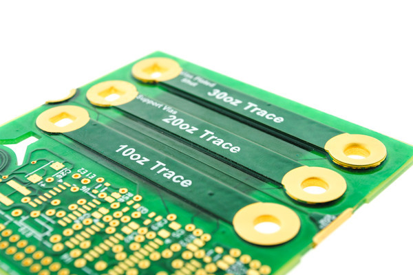
FOWLP (Fan-Out Wafer Level Packaging) represents a significant advancement over traditional packaging approaches. Originally developed by Infineon Technologies , FOWLP was later refined and commercialized by TSMC, which used its proprietary Integrated Fan-Out (InFO) version to secure exclusive production of Apple’s A10 processor for iPhone 7/7Plus in 2016 . This strategic application demonstrated FOWLP’s commercial viability and performance advantages, ultimately displacing Samsung from Apple’s supply chain due to their slower adoption of the technology .
The fundamental innovation of FOWLP lies in its approach to interconnects. Unlike traditional Fan-In WLP, where connections are limited to the chip area itself, FOWLP extends the redistribution layer (RDL) beyond the silicon die perimeter, enabling higher pin counts and improved thermal performance without increasing package size . This “fan-out” approach allows for more I/O connections than would be possible with chip-scale packaging alone.

Technical Advantages and Applications
FOWLP offers several compelling advantages over conventional packaging methods:
•Enhanced Electrical Performance: By eliminating the package substrate and implementing direct RDL connections, FOWLP reduces parasitic effects and shortens circuit paths, resulting in faster signal transmission and reduced power consumption .
•Form Factor Optimization: FOWLP enables thinner profiles and smaller footprints compared to traditional packaging, making it ideal for space-constrained mobile devices .
•Cost Efficiency: The wafer-level processing approach eliminates the need for substrates and wire bonding, potentially reducing production costs by up to 30% while simplifying the supply chain .
These benefits have made FOWLP particularly attractive for mobile applications, where its balance of performance, size, and cost aligns perfectly with industry requirements.
The Evolution to FOPLP Technology
Fundamental Concepts and Value Proposition
FOPLP (Fan-Out Panel Level Packaging) represents a natural evolution of FOWLP principles, scaling the process from round wafers to rectangular panels . This transition from circular to square formats offers fundamental advantages in production efficiency and cost structure. While FOWLP utilizes standard 300mm silicon wafers (approximately 707cm²), FOPLP employs significantly larger panel sizes such as 510×515mm (力成), 600×600mm (日月光), or 610×457mm (approximately 2788cm²) .
The shift in substrate geometry and scale creates substantial benefits:
•Dramatically Improved Area Utilization: Rectangular panels achieve utilization rates of 87-95% compared to approximately 57% for round wafers , effectively reducing wasted peripheral space.
•Increased Production Throughput: A single 610×457mm panel can accommodate approximately four times as many chips as a 300mm wafer , significantly boosting production capacity per processing cycle.
•Enhanced Cost Efficiency: The improved utilization and higher unit output translate to estimated cost savings of 20-30% compared to FOWLP approaches , making FOPLP particularly attractive for high-volume applications.
Technical Implementation Challenges
Despite its compelling advantages, FOPLP implementation faces several technical hurdles:
•Warpage Management: The larger panel format is more susceptible to thermal warpage due to coefficient of thermal expansion (CTE) mismatches between materials . This warpage can affect yield and reliability, requiring advanced materials and process controls.
•Process Uniformity: Maintaining consistent processing conditions across larger panels presents challenges for deposition, lithography, and etching operations, necessitating equipment and material adaptations .
•Material Development: FOPLP requires specialized polymeric materials with optimized thermal, mechanical, and electrical properties to ensure reliability while managing costs .
Current industry reports indicate that these challenges are being successfully addressed, with leading manufacturers achieving trial production yields of approximately 90% for certain applications .
Comparative Analysis: FOWLP vs. FOPLP
Table: Key Technical and Economic Parameters Comparison
| Parameter | FOWLP | FOPLP |
| Substrate Format | Round wafer (300mm/12-inch) | Rectangular panel (510×515mm to 700×700mm) |
| Area Utilization | ~57% | 87-95% |
| Cost Reduction Potential | Baseline | 20-30% vs. FOWLP |
| Technology Maturity | Mature production | Growing adoption, ~90% yield in trials |
| Primary Applications | Mobile processors, RF chips | AI/HPU, automotive, power management ICs |
Market Outlook and Growth Trajectory
The market for fan-out packaging technologies shows significant growth potential, with particularly strong prospects for FOPLP:
•FOPLP Market Expansion: The FOPLP market (including glass substrate packaging) is projected to grow at a 29% CAGR, reaching $29 billion by 2030 , indicating substantial long-term expansion.
•Current Market Position: While FOPLP currently represents a smaller segment of the overall fan-out market (approximately 2% in 2022), its share is expected to increase to 8% by 2028 , reflecting accelerating adoption.
•Polymeric Materials Growth: The broader market for advanced polymeric materials used in these packaging technologies is forecast to grow at a >13% CAGR from 2026 to 2036 , underscoring the material innovation driving these packaging advances.
This growth is fueled by increasing demands from artificial intelligence, high-performance computing, automotive electronics, and 5G/6G communications , all of which require the advanced integration capabilities that FOPLP provides.
Industry Adoption and Key Players
Leading Semiconductor Manufacturers
The development and implementation of FOPLP technology involves major industry players pursuing different strategic approaches:
•TSMC: The industry pioneer in fan-out technologies continues to innovate with both FOWLP (InFO) and developing FOPLP capabilities. The company has established dedicated FOPLP research teams and production lines, with industry observers targeting 2027 for volume production .
•Samsung Electronics: After initially lagging in FOWLP adoption, Samsung has aggressively pursued FOPLP development through collaboration with affiliate Samsung Electro-Mechanics. The company has implemented FOPLP in products including the Galaxy Watch series .
•Intel: While somewhat less focused on FOPLP compared to competitors, Intel has announced breakthroughs in glass substrates for advanced packaging, targeting implementation in the 2026-2030 timeframe .

OSAT and Specialized Providers
The outsourced semiconductor assembly and test (OSAT) sector plays a crucial role in FOPLP development:
•力成 (Powertech Technology): A pioneer in FOPLP implementation, having established the industry’s first FOPLP production line in 2019 . The company offers 510×515mm panel-level solutions with reported yields of approximately 90% .
•日月光 (ASE): Has invested over five years in panel-level solutions, progressing from 300×300mm to 600×600mm panels , with 600×600mm potentially emerging as the industry standard .
•群创 (Innolux): Leveraging panel manufacturing expertise to transition into FOPLP, utilizing approximately 70% of existing panel equipment for packaging applications . The company expects FOPLP to contribute 1-2 percentage points to revenue following volume production .
PCB Industry Implications and Opportunities
Manufacturing Equipment and Process Integration
The rise of FOPLP technology creates significant opportunities for PCB manufacturers with relevant expertise and infrastructure:
•Equipment Adaptation: Approximately 70% of existing panel production equipment can be repurposed for FOPLP applications , potentially lowering barriers to entry for panel manufacturers transitioning to semiconductor packaging.
•Specialized Equipment Development: Companies including 志圣, 均豪, 群翊, 东捷, 晶彩科, 友威科, and 钛昇 are developing specialized tools for FOPLP processes including exposure, development, etching, inspection, and laser processing , representing supply chain opportunities.
•Hybrid Approaches: Some industry leaders are pursuing intermediate solutions such as TSMC’s “COPOS” approach, which implements wafer-level panel packaging for specific applications , suggesting multiple viable paths forward.
Material Science Innovations
Successful FOPLP implementation requires advanced materials addressing key technical challenges:
•Low-Temperature Processes: Development of dielectric polyimides capable of curing at 20-50°C lower temperatures with 50% reduced cure times , essential for managing warpage in large panels.
•Thermal Management: Polymeric materials with optimized coefficient of thermal expansion (CTE) and enhanced thermal conductivity to address warpage and reliability concerns .
•Specialized Formulations: Application-specific material systems balancing competing requirements for low CTE, high thermal conductivity, low dielectric constant, and superior adhesion .
Future Outlook and Strategic Considerations
Technology Development Trajectory
Based on current industry trends and announcements, several developments appear likely in the FOPLP landscape:
•Accelerated Adoption: With major players including NVIDIA and AMD reportedly evaluating FOPLP for upcoming AI processors , volume adoption may accelerate beyond current projections, potentially beginning as early as 2025-2026 .
•Continued Material Innovation: Ongoing development of polymeric materials specifically formulated for panel-level processes will be essential for overcoming current technical barriers, particularly warpage management and thermal performance .
•Standardization Efforts: The current diversity of panel sizes (510×515mm, 600×600mm, 700×700mm) will likely converge toward standardized formats, with 600×600mm emerging as a potential industry standard .
Strategic Recommendations for PCB Manufacturers
For PCB companies considering involvement in the FOPLP ecosystem, several strategic approaches merit consideration:
•Leverage Existing Expertise: Apply PCB manufacturing knowledge in large-panel processing, materials science, and precision patterning to FOPLP challenges.
•Targeted Investment: Focus on specific process steps or materials where PCB industry capabilities provide competitive advantages, such as RDL formation or specialized substrate manufacturing.
•Collaborative Development: Pursue partnerships with semiconductor manufacturers, OSAT providers, and equipment suppliers to develop integrated solutions addressing specific application requirements.
Conclusion: Positioning for the FOPLP Transition
The transition from FOWLP to FOPLP represents a significant evolution in semiconductor packaging, offering compelling advantages in cost structure, production efficiency, and design flexibility. For PCB manufacturers, this shift creates both challenges and opportunities to leverage existing expertise in panel-based processing and advanced materials.
As industry leaders including TSMC, Samsung, and major OSAT providers accelerate FOPLP development and implementation, the technology appears poised for substantial growth, particularly in high-performance applications including AI accelerators, automotive electronics, and next-generation mobile devices. The projected market expansion to $29 billion by 2030 underscores the significant potential of this packaging approach.
For forward-thinking PCB companies, developing capabilities in FOPLP-related processes and materials represents a strategic opportunity to participate in the advanced semiconductor packaging value chain, potentially capturing value in this rapidly evolving segment of the electronics industry.