The layer structure of PCB (printed circuit board) is the core for achieving electrical connections, mechanical fixation, and functional differentiation. The design of different layers directly affects circuit performance, reliability, and manufacturability. According to their functions and purposes, PCB layers can be divided into four categories: electrical layer, auxiliary process layer, mechanical and labeling layer, and special function layer. The following is a detailed analysis of each layer:
Table of Contents
Ⅰ.Electrical layer (core functional layer, realizing signal and power transmission)
The electrical layer is the core layer directly involved in current/signal transmission in PCB, which can be divided into signal layer and inner electrical layer according to position and function, and is the basis for realizing circuit functions.
1. Signal Layers
Used for arranging signal lines and power lines (small current), it is a “wire” that connects component pins. In multi-layer boards, it can be divided into top layer, bottom layer, and middle signal layer.
-Top Layer: The signal layer on the front of the PCB, commonly used for arranging surface mount components (SMT) pads and signal lines, as well as soldering pins for direct insertion components (THD). In a double-layer board, the top and bottom layers are the main wiring layers.
-Bottom Layer: The signal layer on the back of the PCB, which functions similarly to the top layer. In the double-layer board, it needs to be connected to the top layer signal through vias.
-Mid Layers: Only present in multi-layer boards with 4 or more layers (such as Mid1, Mid2, etc.), used for arranging high-density signal lines, reducing the wiring pressure on the top/bottom layers, and especially suitable for impedance control of high-speed signals (such as DDR, PCIe).
Design points:
-Signal lines should avoid sharp turns (recommended ≥ 135 °) to reduce signal reflection;
-High speed signals (such as clock lines) need to be routed separately to avoid interference from power sources/ground layers;
-The signal lines of the same network should be as continuous as possible to reduce the number of vias (which can introduce impedance transients).
2. Internal Plans
Only existing in multi-layer boards, it is a large-area copper layer mainly used for power plan and ground plan, also known as the “power layer” and “ground layer”.
-Power Plan: A power network that connects circuits (such as+5V,+3.3V) to provide stable power supply to components. Large area copper deposition can reduce power impedance and minimize ripple interference.
-Ground Plane: A grounding network (such as GND, AGND) that connects circuits and serves as a “reference ground” for signals. It can absorb noise, shield interference (such as radiation interference from high-frequency signals), and assist in heat dissipation.
Design points:
-The power layer and ground layer need to be arranged adjacent to each other (forming a “power ground plane”), and high-frequency noise should be filtered out using the capacitance effect;
-It is recommended to design analog ground (AGND) and digital ground (DGND) separately to avoid digital signal interference with analog circuits;
-The inner layer needs to be “intact” to avoid large-scale disconnection (unless it is to isolate different power networks), otherwise it will damage the shielding effect.
Ⅱ. Auxiliary process layer (manufacturing and welding assistance)
The auxiliary process layer does not directly participate in electrical connections, but provides guidance for PCB manufacturing, soldering, and testing to ensure production consistency.
1. Solder Mask Layers

Also known as “green oil layer” (common color is green, but can also be customized with black, white, blue, etc.), it is an insulating coating covering the surface of the signal layer to prevent solder short circuits and only expose the solder pads and vias that need to be soldered.
-Top Solder Mask: Covering the top signal layer and exposing the top solder pad;
-Bottom Solder Mask: Covering the bottom signal layer and exposing the bottom solder pads.
Design points:
-The solder mask layer is 0.1-0.2mm larger than the solder pad (“solder mask window”), ensuring that the solder pad is completely exposed;
-Solder Mask Over Via (SMOV) can be set on the via to prevent solder from flowing into the via and causing a short circuit.
2. Paste Mask Layers
Also known as the “steel mesh layer”, it is only used for SMT welding, defining the printing area of solder paste (solder paste), and guiding the position and shape of steel mesh openings.
-Top Paste Mask: Corresponding to the top SMT pad, the steel mesh is perforated according to this layer and solder paste is printed;
-Bottom Paste Mask: Corresponding to the bottom SMT pad, with the same function as above.
Design points:
-The size of the solder aid layer is slightly smaller than the pad (usually 0.05-0.1mm smaller) to avoid solder paste overflow;
-Direct insertion components (THD) do not require the use of soldering layers.
3. Silkscreen Layers
Also known as the “character layer”, it is used for printing component labels, symbols, manufacturer information, etc., facilitating soldering, debugging, and maintenance.
-Top Silkscreen: printed on the surface of the top solder mask layer, marking the top components (such as R1, C2, IC model);

-Bottom Silkscreen: Printed on the surface of the bottom solder mask layer, marking the bottom components (text needs to be mirrored to ensure it is viewed from the front).
Design points:
-The characters should be clear and visible (recommended line width ≥ 0.15mm, height ≥ 1mm), avoiding covering the solder pads (otherwise affecting soldering);
-Polarized components (such as capacitors and diodes) need to be labeled with polarity symbols (+/-, directional arrows).
Ⅲ. Mechanical and Annotation Layer (Defining Physical and Information Attributes)
Used to define the physical boundaries, installation structure, and additional information of PCB, ensuring mechanical dimensions and assembly compatibility.
1. Mechanical Layers
-Outline layer (usually Mechanical 1): defines the physical dimensions of PCB such as outline (border), rounded corners, and slots, and is the “cutting basis” for PCB processing.
-Installation hole layer: Mark the position and size (such as diameter and tolerance) of screw holes and positioning holes to ensure compatibility with the housing/bracket.
-Remarks layer: Mark the material (such as FR-4), thickness (such as 1.6mm), tolerance (such as ± 0.1mm), version number, and other information of the PCB for easy production and traceability.
Design points:
-The outer layer needs to be closed to avoid processing errors caused by “broken edges”;
-The distance between the installation hole and the components and signal lines should be ≥ 0.5mm to prevent mechanical stress damage to the circuit.
2. Drill Layers
Guide drilling processing, clarify the type, location, and size of the holes.
-Drill Guide: Mark the center position and coordinates of the drill hole;
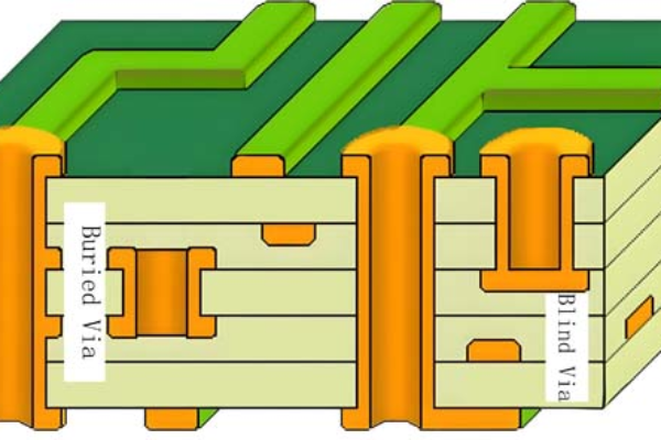
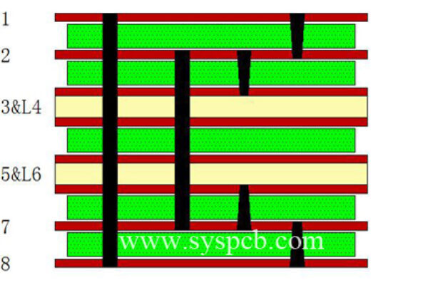
-Drill Drawing: Summarize the dimensions (e.g. 0.8mm, 3.0mm), types (through-hole, blind hole, buried hole), and quantities of all holes to generate a Drill Table.
Design points:
-The diameter of the via hole needs to match the wire (e.g. 0.2mm line width corresponds to 0.3mm via hole);
-Blind/buried holes need to be marked with depth (e.g. “Blind hole: top layer → Mid1, depth 0.8mm”).
Ⅳ.Special functional layer (targeted design requirements)
Used for constraints or isolation in specific scenarios to ensure circuit performance.
1. Prohibit wiring layer (Keep Out Layer)
Define the “wiring exclusion zone” of the PCB, which prohibits the placement of components, signal lines, or vias within the boundary of that layer. It usually overlaps with the outer layer (to prevent wiring from exceeding the PCB range) and can also be used to isolate sensitive areas (such as RF modules).
2. Prohibit placing layers (Keep In Layer)
Contrary to the prohibition of wiring layers, the definition of “only allowing placement of components or wiring within this area” is used to limit the layout range of components (such as PCBs in narrow spaces).
3. Mixed Layer
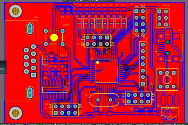
Display a stacked view of all layers for easy inspection of positional conflicts (such as silk screen covering solder pads, overlapping vias and mounting holes).
Examples of Layer Structures for PCBs with Different Layers
-Double layer board: top layer (signal), bottom layer (signal)+top layer solder mask, bottom layer solder mask+top layer silk screen, bottom layer silk screen+mechanical layer (appearance), drilling layer, prohibited wiring layer.
-Four layer board: top layer (signal), bottom layer (signal)+Mid1 (signal)+inner layer 1 (ground), inner layer 2 (power supply)+the above auxiliary layer and mechanical layer.
Summarize
The layer structure of PCB is an organic combination of “electrical function+process assistance+mechanical constraints”:
-The electrical layer (signal layer, internal electrical layer) determines the connection and performance of the circuit;
-The auxiliary process layer (solder mask, soldering aid, silk screen printing) ensures the reliability of manufacturing and welding;
-Mechanical and special layers define physical properties and design constraints.
Reasonably planning the functions of each layer is the key to achieving high-density and high reliability PCB design.
Get your exclusive quote immediately: fill out the form or send an email directly.As a professional PCB manufacturer for hobbyist , we will provide you with a quote service within 24 hours. Enjoy free DFM optimization and a 10% discount on SMT patches for your first order!