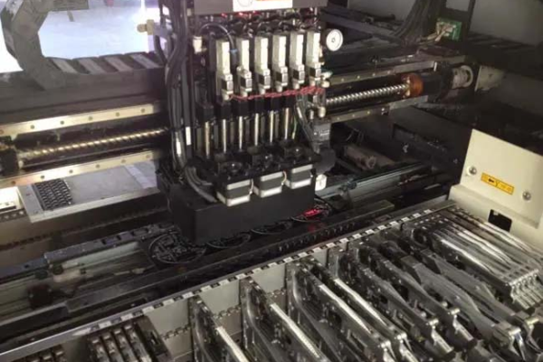
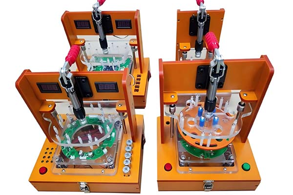
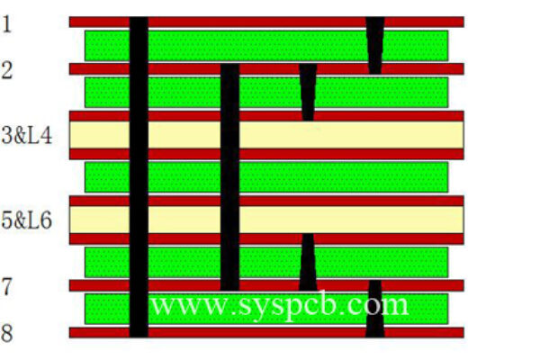
In PCB manufacturing, the process of panelization is essential for optimizing production efficiency. Since PCBs are often produced in panels containing multiple individual boards, panelization techniques determine how the boards are separated after assembly and testing. Two common methods for circuit board panelization are V-scoring and tab routing. Both methods have their advantages and limitations, and choosing the right technique depends on factors like design complexity, material type, and cost considerations. In this blog post, we will explore these two methods in detail, helping you understand their differences and applications.
Table of Contents
What is Panelization?
Panelization refers to the process of arranging multiple individual PCB designs onto a larger panel for efficient manufacturing, including processes like soldering, testing, and inspection. Once the PCBs are assembled and tested, they need to be separated into individual boards. Panelization methods help achieve this separation while ensuring the structural integrity of the PCBs and minimizing production time.
V-Scoring: The Basics
V-scoring is one of the most widely used panelization methods, especially for single-sided PCBs. In this method, a “V” shaped groove is milled into the panel along the lines where the individual PCBs will be separated. The groove is typically shallow, leaving the board mostly intact except for a thin, scored section that allows for easy breakage along the scored lines.
Advantages of V-Scoring
Cost-Effective: V-scoring is generally more cost-effective than other methods, especially for simpler designs. The process involves creating shallow cuts along the panel edges, which reduces the need for additional complex machining.
Efficiency: Since the scored lines are relatively easy to create, this method is ideal for mass production. The scored panel can be easily snapped apart after the assembly process, speeding up the overall manufacturing workflow.
No Extra Material Waste: The V-scoring process doesn’t involve any extra material removal beyond the groove, reducing waste and making it more environmentally friendly.
Minimal Impact on Component Placement: Because the scoring is shallow, it doesn’t affect the placement of components on the board or the routing of traces, making it ideal for densely populated designs.
Limitations of V-Scoring
Limitations for Complex Shapes: V-scoring is best suited for rectangular or simple shapes. For PCBs with complex geometries or irregular edges, this method may not be feasible or effective.
Risk of Breakage: If the V-scoring is not executed correctly, it can weaken the PCB and increase the risk of breakage during manufacturing or handling, especially for fragile designs.
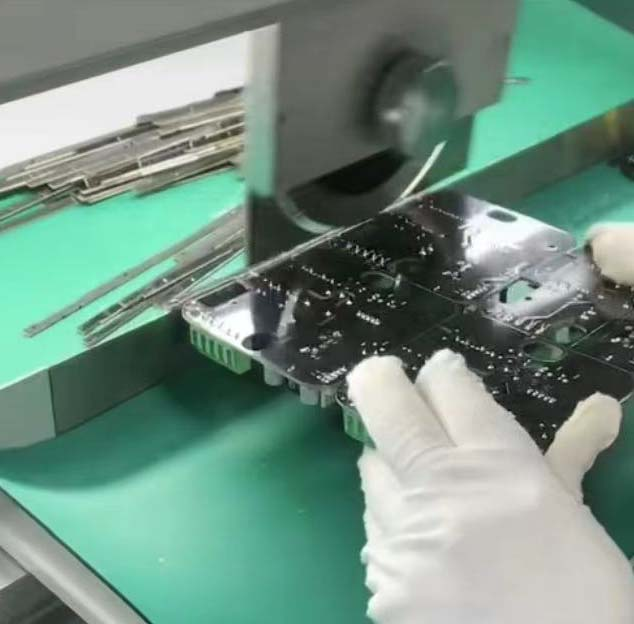
Tab Routing: The Basics
Tab routing involves creating individual PCBs within a larger panel and then connecting them with “tabs”—small sections of material that hold each PCB in place during the manufacturing process. Once the boards are fully assembled, these tabs are cut or broken to separate the individual PCBs.
Advantages of Tab Routing
Versatility: Tab routing is ideal for more complex PCB designs, especially those with irregular shapes or intricate edge patterns. Since the PCBs are separated by tabs, this method allows for more design flexibility.
Reduced Risk of Damage: The tabs act as mechanical supports, which can help reduce the risk of damage to the PCBs during manufacturing and handling. This is particularly important for designs with sensitive components or thin substrates.
No Risk of Over-Scoring: With tab routing, there’s no need to worry about over-scoring or damaging the PCB surface, which can sometimes occur with V-scoring if the cuts are too deep.
Limitations of Tab Routing
Higher Cost: Tab routing generally involves more complex machining and may require additional steps for tab removal. As a result, this method tends to be more expensive than V-scoring, especially for mass production.
Material Waste: Since tabs are cut from the panel, there can be more material waste compared to V-scoring, especially in designs with many tabs and larger panels.
Increased Handling Complexity: The process of removing tabs can require additional handling and equipment, potentially increasing the time and labor needed to separate the individual PCBs.
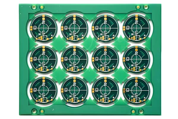
V-Scoring vs Tab Routing: Which to Choose?
The decision between V-scoring and tab routing depends largely on the specific needs of the PCB design and manufacturing process. Here’s a quick comparison:
| Factor | V-Scoring | Tab Routing |
| Cost | Lower cost, ideal for high-volume production | Higher cost due to additional steps and machining |
| Design Flexibility | Limited to simpler, rectangular designs | More flexibility for complex or irregular shapes |
| Production Efficiency | High efficiency for simple designs | May require more time and effort for tab removal |
| Material Waste | Minimal, no additional material removal | Higher waste due to tab cutting |
| Risk of Damage | Risk of breakage if scored improperly | Reduced risk, as tabs hold the boards in place |
| Use Case | Best for high-volume, simple designs | Ideal for intricate, custom, or low-volume designs |
Conclusion
Both V-scoring and tab routing offer distinct advantages depending on the type of PCB design and the specific manufacturing requirements. V-scoring is an economical choice for simpler, high-volume designs with minimal risk of damage, making it suitable for mass production of rectangular or straightforward boards. On the other hand, tab routing provides more flexibility for complex, irregular shapes, offering better protection against breakage at a higher cost.
Ultimately, the choice between these panelization methods should be based on the design’s complexity, production volume, and budget constraints. By understanding the strengths and weaknesses of each method, you can make an informed decision to optimize the PCB manufacturing process and ensure the quality and efficiency of your final product.


