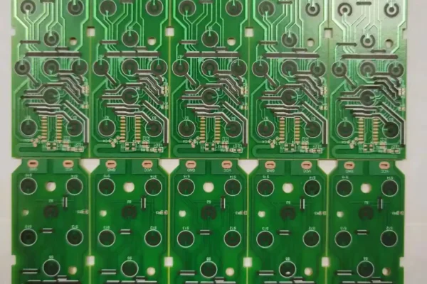
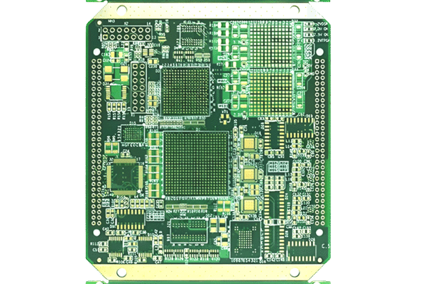
In the world of electronics manufacturing, Surface Mount Technology (SMT) is one of the most widely used techniques for assembling electronic components onto PCBs (Printed Circuit Boards). SMT has revolutionized the way electronic devices are designed and produced, offering numerous benefits over traditional through-hole mounting methods.
There are roughly four steps in the process of SMT processing: solder paste printing → component placement → reflow soldering → AOI.
Of course, it can be further subdivided: feeding → solder paste printing (side A) → component placement (side A) → visual inspection in front of the reflow soldering → reflow oven → solder paste printing (side B) →component placement (side B) →visual inspection in front of the reflow soldering → reflow oven → inspection after reflow soldering →split board → download → FQA inspection → production inspection → FT test → BT test → CIT test
Each step is described in detail below:
Table of Contents
1. Feeding

Feeding means that after the factory receives the customer’s BOM, the corresponding program will be written, and then the item number and item name will be listed in the corresponding machine. At this time, the warehouse can arrange the materials of the project to be produced in advance according to the plan, and then the material production personnel will put the materials into the corresponding machine according to the material number set in the machine. After the production material personnel have loaded the materials, the inspectors will coordinate to check whether there is any inconsistency in the material numbers, and sign the material on the material feeding record. PQA will randomly check the material feeding situation when patrolling the line.
1.1 When a plate of materials is used up and a new plate needs to be replaced, it will be placed in the wrong place if the personnel do not pay attention. At present, all materials are required to be confirmed by both the production staff and the inspector before going online.
1.2 When the incoming part number is handwritten, there will be quality risks. The handwritten part number itself may be wrong, and the person checking the part number may mistake the part number for another part number.
1.3 Some production reject parts are not easy to distinguish when they are recycled, need to define the time used up.
1.4 When the material is relatively small and needs to be patched separately at each station, the corresponding personnel are required to confirm when reposting the label.
2. Solder paste printing

The solder paste must be warmed before use, and the opening time must be recorded after opening and must be stirred evenly before it can be used online. At present, the control method of solder paste control printing is an important parameter to record the printing results, which cannot be deviated from the defined range, that is, blade pressure, demolding speed, demoulding distance, printing speed, automatic cleaning frequency, automatic cleaning speed, etc. OP’s request is two hours of cleaning, manual cleaning of the stencil once, and a cleaning record.
The final monitoring method for the effectiveness of the solder paste machine is to measure whether the thickness of the solder paste is within the standard range, and use the CPK value to monitor the effectiveness of the MPM/DEK. However, the monitoring method for the solder paste offset is only to have the OP look at the magnifying glass, and if the board has problems such as continuous soldering and offset after reflow soldering, it will go back to investigate whether the solder paste printing is the problem.
2.1 The solder paste is not used as required.
2.2 The printing problems were not fed back to the relevant personnel in time for adjustment.
2.3 Although the height of the solder paste after printing meets the requirements of the range, when CPK1.67 or 7 points in a row is on one side of the center line, the employees fail to report the problem in time. Even after the problem is reported, the relevant craftsmen are not sure how to adjust it.
3. Component placement
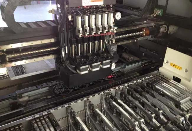
The component feeder and the PCB are fixed. The placement head moves back and forth between the feeder and the PCB, and the components are taken out from the feeder. After adjusting the position and orientation of the components, they are placed on the PCB.
3.1 When some holes of the suction nozzle are blocked, and the appearance and color of the material are different, it will cause the machine to throw material and so on.
3.2 When the material belt is not placed horizontally, the material belt is broken, and the viscosity is too high, which is blamed on the supplier.
3.3 When the incoming material is inconsistently placed in the material belt, or the incoming material does not match the size of the material tray, it will also affect the quality of the patch.
3.4 The person inspecting before the reflow soldering should be able to supervise the problem. If it is above the 0603 level, a little offset will not affect the product quality, but if it is a 0.5PIN component, in principle, no offset is allowed.
4. Reflow soldering

In the process of hot air reflow soldering, the solder paste needs to go through the following stages, the solvent is volatilized; the flux removes the oxides on the surface of the soldered parts; the solution of the solder paste is reflowed to cool and solidify the solder paste.
4.1 Preheating zone
Preheat the PCB and components to achieve equilibrium, while removing moisture and solvent volatilization in the solder paste. It is relatively mild, and the thermal shock to the components is as small as possible. If the temperature rises too fast, it will cause damage to the components, such as cracking of the multilayer ceramic capacitor. At the same time, it will also cause solder spatter, resulting in the formation of solder balls and insufficient solder joints in the non-soldered areas of the entire PCB.
4.2 Heat preservation area
Ensures that the solder is completely dry before reaching the reflow temperature, and also acts as flux activation to remove metal oxides from components, pads, and solder powder. The time is about 60~120 seconds, depending on the properties of the solder.
4.3 Reflow area
The solder in the solder paste causes the gold powder to begin to melt and flow again, replacing the liquid flux to wet the pads and components. This wetting action causes the solder to spread further, with a wetting time of 60 to 90 seconds for most solders. The temperature of reflow soldering should be higher than the melting point temperature of solder paste, generally 20 degrees higher than the melting point temperature to ensure the quality of reflow soldering. This area is also sometimes divided into two zones, the melt-off and reflow zones.
4.4 Cooling area
The solder solidifies as the temperature decreases, so that the components and the solder paste form a good electrical contact, and the cooling speed should not be too different from the preheating speed.
5. Split board
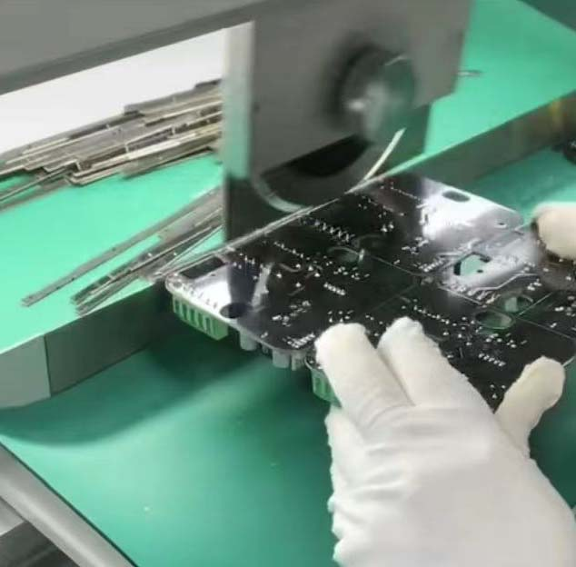
At present, a splitting machine is used, which adopts rotary cutting, but sometimes the factory will cut the auxiliary board by hand with scissors due to production capacity. When it is necessary to cut by hand, a document is formulated to inform the OP of the cutting order, and when the cutting is completed, the effect of the inspection is to prevent the phenomenon that the last part of the board edge is broken by hand.
6. Test
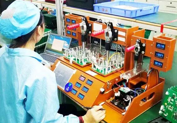
Once the PCB has passed inspection, it goes through testing to ensure it functions as intended. Common types of testing include:
In-Circuit Testing (ICT): Checks for correct component placement and electrical functionality.
Functional Testing (FCT): Tests the PCB in a real-world operating environment to verify that it meets the required performance specifications.
7. Inspection
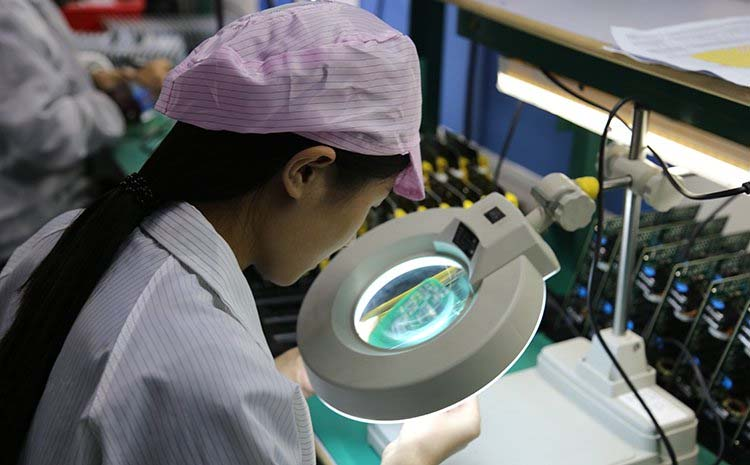
After the soldering process, the assembled PCB undergoes various inspection processes to ensure that all components are correctly placed and soldered. There are several ways to inspect the board:
Visual Inspection: Technicians check the board for visible defects such as misalignment, poor solder joints, or missing components.
Automated Optical Inspection (AOI): AOI machines use cameras and advanced algorithms to inspect the PCB for defects and ensure component placement accuracy.
X-ray Inspection: For more complex boards with hidden solder joints (such as BGAs – Ball Grid Arrays), X-ray inspection is used to ensure the integrity of the solder joints.
Once the PCB passes all tests, it undergoes a final inspection to ensure it meets all design and quality standards. The board is then cleaned, packaged, and prepared for shipment to the next stage in the manufacturing process or for final assembly.
Hot Tags: SMT Process manufacturer, Split board manufacturing services, Solder paste printing manufacturing, pcb board assembly suppliers, Inspection PCB, surface mount technology, SMT processing, Test PCB, reflow soldering, Customized Component placemen, factory, quotation, cheap