Table of Contents
Introduction: The Transformative Shift in PCB Technology
The printed circuit board (PCB) industry is undergoing a fundamental transformation, moving from a simple component provider to a critical enabler of technological innovation. According to TrendForce, 2026 will mark a new starting point where PCB value is driven by technical content rather than just production volume . This shift is primarily fueled by the explosive growth in artificial intelligence (AI), which has created unprecedented demands for higher performance, greater density, and enhanced reliability in electronic systems.
High-end PCBs represent the cutting edge of this evolution, incorporating advanced materials, sophisticated designs, and precision manufacturing processes to meet the rigorous requirements of modern AI infrastructure, automotive electronics, and high-performance computing. As AI servers alone demonstrate PCB usage 50-60 times greater than traditional servers, the industry faces both tremendous opportunities and significant challenges in scaling these complex technologies .
This comprehensive guide explores the technical specifications, market dynamics, and future trends shaping the high-end PCB landscape, providing valuable insights for businesses navigating this rapidly evolving sector.
1 The AI Revolution: Redefining PCB Requirements
1.1 Structural Shifts in AI Server Design
AI server architecture is undergoing fundamental changes that directly impact PCB design and functionality:
•Cableless Interconnect Designs: NVIDIA’s Rubin platform eliminates traditional cabling between GPU and Switch components, replacing them with sophisticated multi-layer PCB trays including Switch trays, Midplanes, and CX9/CPX interfaces that must maintain exceptional signal integrity (SI) and transmission stability .
•Increased Layer Counts: AI server motherboards have evolved from traditional 12-layer designs to complex configurations ranging from 40 to over 50 layers, with some specialized projects implementing 56-layer designs (M+N layered structures) to accommodate dense interconnects .
•Material Upgrades: To achieve low loss and low latency, Rubin platform components utilize advanced materials including M8U grade (Low-Dk2 + HVLP4) for Switch trays and M9 (Q-glass + HVLP4) for Midplane and CX9/CPX boards, with some configurations reaching up to 104 layers .
1.2 Explosive Growth in AI PCB Demand
The demand surge for high-end PCBs in AI applications is unprecedented:
•Volume Increase: AI servers require approximately 50-60 times more PCB content compared to traditional servers, creating massive supply chain pressures .
•Value Enhancement: Single AI servers now deliver over twice the PCB value of previous generations, reflecting their increased complexity and advanced material content .
•Market Expansion: The AI infrastructure market is projected to grow from approximately $60 billion to nearly$500 billion over the next decade, ensuring sustained demand for high-end PCB solutions .
Table: AI Server PCB Requirements Compared to Traditional Servers
| Parameter | Traditional Servers | AI Servers | Key Implications |
| PCB Layer Count | 12-16 layers | 40-56+ layers | Increased design and manufacturing complexity |
| Material Requirements | Standard FR-4 | Low-loss laminates (M8U, M9) | Higher cost, specialized supply chain |
| Thermal Design Power | Hundreds of watts | Over 2,000W | Advanced thermal management solutions |
| PCB Value per Server | Baseline | 2x+ higher | Improved margins for capable manufacturers |
| Supply Chain Model | Standard inventory | Constrained specialty materials | Strategic inventory management required |
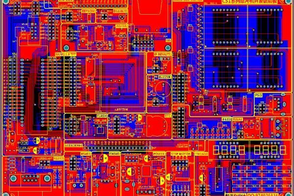
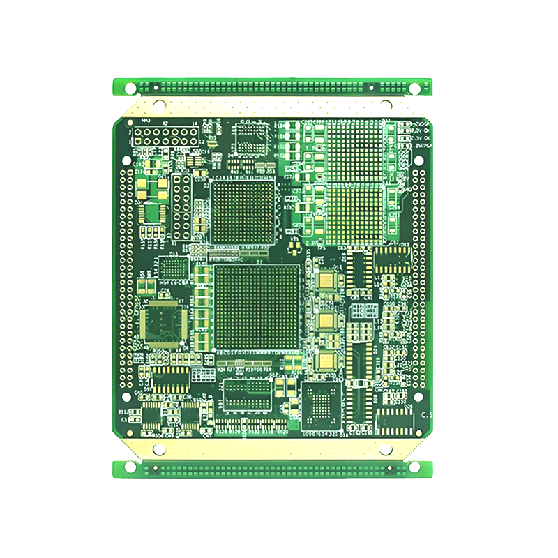
2 Technical Specifications of High-End PCBs
2.1 Advanced Material Systems
The performance of high-end PCBs is fundamentally linked to their material composition:
•Specialized Glass Fabrics:
–T-glass: Features low thermal expansion coefficient and high modulus characteristics, making it essential for ABF and BT substrates. With prices several times higher than standard E-glass, production is expanding with Nittobo investing ¥15 billion to triple production capacity by late 2026 .
–Q-glass: Offers extremely low dielectric constant and minimal dielectric loss, becoming the future direction for high-speed applications .
•Copper Foil Innovations:
–HVLP4 copper foil has become the standard for high-speed applications due to its low roughness profile, which minimizes skin effect losses at high frequencies .
–Each upgrade in roughness class reduces production capacity by approximately half, creating long-term supply constraints and shifting pricing power upstream to material suppliers .
•Dielectric Materials: Progression toward carbon hydrogen and PTFE-based resins that provide lower dielectric constants and reduced signal loss, replacing traditional epoxy systems in critical applications .
2.2 Manufacturing Process Innovations
Producing high-end PCBs requires specialized manufacturing approaches:
•mSAP (modified Semi-Additive Process): This advanced fabrication technique enables the creation of circuits with line widths below 10μm, essential for high-density interconnects in AI processors and advanced packaging applications .
•Panel-Level Packaging: Technologies like Chip-on-Wafer-on-Panel (CoWoP) are emerging as potential future packaging routes, using large-format PCB panels to directly mount multiple chips, thereby reducing costs while improving interconnect density .
•Laser Direct Imaging & Drilling: Advanced laser systems enable finer trace widths and microvias with diameters below 75μm, required for high-density interconnects in AI server processors .
3 Market Dynamics and Supply Chain Challenges
3.1 Structural Supply-Demand Imbalance
The high-end PCB market is characterized by significant supply constraints:
•Capacity Limitations: Only a limited number of global manufacturers possess the capability to reliably produce 18+ layer PCBs with the required precision and consistency, creating a structural shortage .
•Material Shortages: Key materials including T-glass fiber cloth and high-grade copper-clad laminates (CCL) face extended supply deficits, with constraints expected to persist through 2026 .
•Extended Qualification Cycles: The development and validation cycle for new high-end glass fabrics exceeds two years, preventing rapid capacity expansion to meet surging demand .
3.2 Geographic Production Trends
The global PCB production landscape is evolving in response to market pressures:
•Southeast Asian Expansion: Taiwanese and Chinese PCB manufacturers are actively establishing production facilities in Thailand to diversify manufacturing footprints, though these efforts face challenges including workforce development and infrastructure scaling .
•U.S. Manufacturing Initiatives: EMS providers are initiating U.S.-based manufacturing operations, potentially reshaping global trade patterns for high-reliability applications .
•Copper Price Volatility: Fluctuating copper prices combined with international geopolitical tensions present ongoing challenges for cost management and production planning .

4 Emerging Applications Driving Demand
4.1 AI Hardware Infrastructure
Beyond traditional servers, multiple AI hardware segments require advanced PCBs:
•GPU Accelerator Boards: High-performance computing cards demand ultra-high layer counts and sophisticated thermal management to support processors exceeding 2000W TDP .
•Network Switching Systems: AI cluster networking components require extreme signal integrity with 112G SerDes and beyond, necessitating ultra-low loss materials and precise impedance control .
•Advanced Packaging Substrates: As chiplet-based architectures gain prominence, the line between PCBs and semiconductor packaging blurs, with substrates growing from 150×150mm to over 200×200mm to accommodate advanced packaging schemes .
4.2 Automotive Electronics
The automotive sector represents another high-growth market for advanced PCBs:
•ADAS Systems: Advanced driver assistance systems typically require 12+ layer HDI boards with exceptional reliability to handle sensor fusion processing in safety-critical applications .
•Electric Vehicle Powertrains: 800V+ electrical systems demand specialized high-thermal conductivity substrates capable of managing substantial power loads while maintaining electrical isolation .
•Zero-Defect Requirements: Automotive applications enforce rigorous quality standards with expectations of flawless operation across extreme environmental conditions and multi-year service life .
5 The Future Outlook: Technology Roadmap
5.1 Material Science Innovations
Ongoing material development will continue to enable PCB performance improvements:
•Low Thermal Expansion Materials: Next-generation substrates with reduced Z-axis CTE will enhance reliability during thermal cycling, particularly important for large-format boards .
•Thermal Management Integration: Substrates increasingly incorporate thermal management functionality, integrating heat spreaders and sometimes integrated voltage regulators (IVRs) to support high-power components .
•Sustainable Material Options: Growing emphasis on halogen-free and environmentally compatible material systems that maintain performance while addressing regulatory requirements .
5.2 Manufacturing Technology Evolution
Production methodologies continue to advance to support increasing complexity:
•Additive Processes: Expanded adoption of mSAP and related additive techniques to achieve finer feature sizes below 20μm line/space requirements .
•Hybrid Structures: Integration of different material types within single board constructions to optimize performance characteristics while managing costs .
•AI-Optimized Manufacturing: Implementation of AI and machine learning systems to enhance production yield, predict maintenance needs, and optimize process parameters in real-time .
6 Strategic Implications for PCB Manufacturers
6.1 Capability Development Priorities
To compete effectively in the high-end PCB market, manufacturers should focus on several key areas:
•Material Expertise: Develop deep understanding of specialized material properties and their interaction with manufacturing processes to optimize performance and yield .
•Advanced Process Controls: Implement rigorous process monitoring and control systems to maintain consistency across complex multi-stage manufacturing sequences .
•Supply Chain Diversification: Establish multiple sourcing options for critical materials to mitigate shortage risks while maintaining quality standards .
6.2 Business Model Evolution
Success in the high-end segment requires strategic business adaptations:
•Collaborative Development: Engage early with customers during design phases to optimize designs for manufacturability while meeting performance requirements .
•Technology Roadmapping: Maintain clear visibility into emerging application requirements to align capital investments and R&D initiatives with future market needs .
•Value-Based Positioning: Transition from commodity pricing to value-based models that reflect the sophisticated engineering and specialized capabilities required for advanced PCB production .
Conclusion: Positioning for the High-End PCB Era
The high-end PCB market represents both a tremendous opportunity and significant challenge for the electronics industry. As AI, automotive, and computing applications continue to drive requirements for higher layer counts, advanced materials, and sophisticated designs, manufacturers capable of mastering these complex technologies will capture disproportionate value.
The transition from volume-based to technology-content-driven value highlighted by TrendForce underscores the fundamental shift underway in the PCB industry . Companies that invest in developing deep materials expertise, precision manufacturing capabilities, and collaborative customer relationships will be best positioned to thrive in this evolving landscape.
With the AI infrastructure market projected to expand nearly tenfold over the next decade , the strategic importance of high-end PCBs will only increase. Manufacturers who embrace this technological transformation today will become the industry leaders of tomorrow, powering the next generation of electronic innovation across AI, automotive, and beyond.