Table of Contents
Introduction
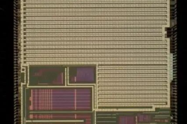
In the competitive landscape of printed circuit board (PCB) manufacturing, implementing a thorough design verification process significantly reduces errors, prevents costly re-spins, and accelerates time-to-market. A comprehensive PCB design checklist serves as a critical quality assurance tool, systematically addressing potential issues across design data integrity, electrical functionality, physical layout, and manufacturing readiness.
This guide consolidates essential verification steps from industry best practices, providing PCB engineers and designers with a structured framework to ensure their designs are optimized for performance, reliability, and manufacturability before release to production.
1 Design Data and Documentation Verification
1.1 Input Data Completeness
Before commencing PCB layout, verify that all input documentation is complete and current:
•Confirm receipt of latest schematic diagrams, board layout files (.brd), bill of materials (BOM), and PCB design specifications
•Validate template positioning devices and mechanical reference points are accurately placed
•Ensure keep-out zones from mechanical drawings are properly represented in the PCB template
•Cross-reference board outline dimensions and tolerances against mechanical drawings, confirming accurate definition of plated vs. non-plated holes
1.2 Documentation Accuracy
•Verify PCB design requirements, standardization specifications, and change requests are clearly documented and implemented
•Once confirmed, lock the structural files to prevent accidental movement
•Ensure assembly drawings clearly indicate polarity, component orientation, and test points

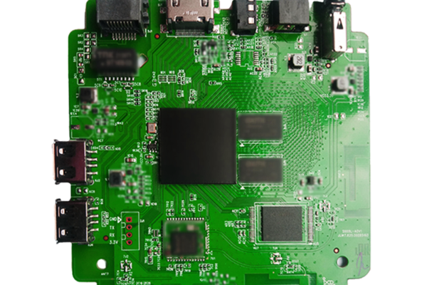
2 Component Placement Verification
2.1 Library Management and Physical Clearances
•Confirm all component footprints match the authorized library versions
•Verify board-to-board connections have correct signal mapping, connector orientation, and silkscreen identification
•Ensure 100% component placement completion
•Check for DRC violations from component overlaps by examining TOP and BOTTOM place-bound layers
•Validate fiducial markers are sufficiently placed where needed
2.2 Mechanical and Thermal Considerations
•Position heavier components near PCB support points or edges to minimize board warpage
•Lock mechanically critical components after placement to prevent accidental movement
•Maintain clearance around press-fit connectors (typically 5mm) from taller components on opposite sides
•Ensure heat-sensitive components (including liquid dielectric capacitors and crystals) are adequately separated from high-power devices and heat sinks
•Verify component placement accommodates thermal management requirements and heat dissipation paths
2.3 Signal Integrity and EMC Layout
•Separate digital and analog circuits with appropriate partitioning
•Position A/D converters to bridge analog and digital sections
•Place clock generation circuits optimally for shortest and cleanest signal distribution
•Locate high-speed devices to minimize signal path lengths and disruptions
•Verify termination components are correctly positioned (source termination near drivers, end termination near receivers)
•Ensure decoupling capacitors are adequate in quantity and positioned close to IC power pins
•Confirm signal reference plane transitions have appropriate coupling capacitors near crossing points
3 Routing and Electrical Verification
3.1 Signal Integrity and High-Speed Routing
•Maintain consistent impedance for high-speed signals across layers
•Ensure differential pairs are routed with proper length matching, symmetry, and parallel alignment
•Route clock signals on internal layers whenever possible, referenced to solid ground planes
•Apply 3W rule (space between traces ≥ 3x line width) for clock, high-speed, reset, and other sensitive signals to minimize crosstalk
•Avoid routing high-speed signals through dense via regions or between component pins
•Confirm all differential pairs and high-speed buses meet signal integrity constraints
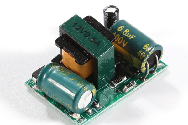
3.2 Power Distribution Network
•Verify IC power connections are not excessively long or indirect
•Check LDO and power module surrounding circuitry layout appropriateness
•Ensure overall power distribution provides adequate current capacity with minimal voltage drop
•Confirm power/ground plane splits don’t create problematic return paths for high-speed signals
•Validate power traces are sufficiently wide for expected current loads (using standards such as 1A/mm for outer layers, 0.5A/mm for inner layers)
3.3 EMC and Reliability Enhancements
•Place a ground plane underneath crystals and avoid signal lines passing between device pins
•Eliminate sharp angles and 90-degree turns in signal traces (use 135-degree angles or curved traces)
•Route high-speed signals adjacent to their return paths (tight to ground planes in multilayer boards)
•Orient adjacent layer traces perpendicular to each other when possible to reduce crosstalk
•Avoid routing signals underneath power modules, common-mode chokes, transformers, or filters
•Minimize long parallel runs of high-speed signals on the same layer
•Add shield vias along ground plane splits, with spacing less than λ/20 of the highest frequency
•Ensure no isolated copper islands, excessive slots, or severe fractures in power and ground planes
4 Manufacturing and Assembly Preparation
4.1 Design Rule Implementation
•Confirm all signal integrity constraints are properly defined in the constraint management system
•Verify appropriate settings for physical and electrical rules, particularly for power and ground networks
•Ensure adequate spacing for test vias and test points
•Validate layer stack-up configuration meets impedance control requirements and manufacturer capabilities
4.2 Solder Mask and Silkscreen
•Confirm solder mask clearance around pads is sufficient to prevent bridging (typically ≥2mil)
•Verify silkscreen legibility with minimum text height (≥0.8mm) and line width (≥8mil), avoiding placement over pads
•Ensure component reference designators are visible, accurate, and properly oriented
•Validate pin 1 indicators, polarity markings, and connector identifications are clear and correct
•Check for proper board identification including part numbers, revision codes, and dates
4.3 Panelization and Board Finishing
•If panelization is required, ensure routing tabs, breakaway tabs, or v-scoring meet manufacturer specifications
•Verify board edge clearance for copper and traces (typically ≥0.5mm, recommended ≥2mm)
•Confirm internal ground planes extend slightly beyond board edges (1-2mm recommended)
•Check non-plated holes maintain adequate clearance from internal copper (≥0.5mm)

5 Output File Generation and Verification
5.1 Drill Documentation
•Verify PCB thickness, layer count, silkscreen color, and other technical notes in drill drawing
•Confirm stack-up layer names, material thicknesses, and copper weights are accurately documented
•Ensure impedance control requirements are clearly specified if applicable
•Generate updated drill files after any hole modifications
•Check hole size table for anomalies and verify press-fit hole sizes are correctly defined
•Identify filled vias in separate callouts if required
5.2 Gerber File Generation
•Output Gerber files in RS-274X format with 5:5 precision
•Generate updated aperture files unless using 274X format
•Review Gerber generation logs for any anomaly reports
•Inspect negative layers for isolated islands and proper clearances
•Use Gerber verification tools to compare output files against original PCB layout
5.3 Documentation Package
•Ensure complete manufacturing package includes:
–PCB layout files with proper version identification
–Gerber files for all signal, power, mask, and silkscreen layers
–NC drill files with proper formatting
–SMT assembly data with component coordinates
–Test files for flying probe or bed-of-nails testers
–Mechanical reference files in standardized formats
6 Design for Manufacturing (DFM) and Testing
6.1 Manufacturing Compliance
•Verify trace widths/spacing meet manufacturer capabilities (typically ≥3-4mil)
•Confirm hole sizes respect aspect ratio limitations (typically 8:1 for plated through-holes)
•Check solder mask bridges between fine-pitch components are within manufacturer limits
•Validate copper pour clearances to board edges meet fabricator requirements
6.2 Testability Verification
•Confirm adequate test point access for key signals (power, ground, clocks, reset)
•Ensure test point spacing accommodates target test equipment (typically ≥2.54mm)
•Verify component heights don’t obstruct test probe access
•Check BGA devices have accessible test points via vias if direct probing isn’t feasible
Conclusion
Implementing a systematic PCB design verification process using this comprehensive checklist significantly enhances manufacturing success rates, reduces development costs, and improves product reliability. By methodically addressing data integrity, component placement, signal integrity, power distribution, manufacturing requirements, and documentation accuracy, PCB professionals can confidently release designs to production with minimal risk of respins or field failures.
The most effective verification processes combine automated design rule checking with meticulous manual review of application-specific requirements, creating a robust framework for delivering high-quality PCB designs across diverse technologies and complexity levels.