Table of Contents
Introduction to PCB Lamination
PCB lamination – also known as layer pressing or multilayer lamination – represents one of the most critical processes in multilayer printed circuit board manufacturing. This sophisticated procedure involves bonding inner layer cores, prepreg (B-stage) insulation layers, and copper foils under controlled temperature and pressure to form a solid, reliable multilayer structure. As electronic devices continue evolving toward miniaturization and higher performance, the importance of advanced lamination technologies has grown significantly, with modern PCB designs requiring increasingly complex multilayer configurations to accommodate dense component placement and high-speed signal transmission.
The lamination process fundamentally transforms discrete materials into a unified composite structure that must maintain electrical integrity, mechanical stability, and thermal reliability throughout the product’s operational life. According to industry literature, “The technology of laminating of multilayer PCB determines quality of PCB”, highlighting the process’s crucial role in determining final board quality. This comprehensive guide explores the technical specifications, material considerations, process variations, and quality control measures that define successful PCB lamination in modern electronics manufacturing.
1.The Fundamental Principles of PCB Lamination
What is PCB Lamination?
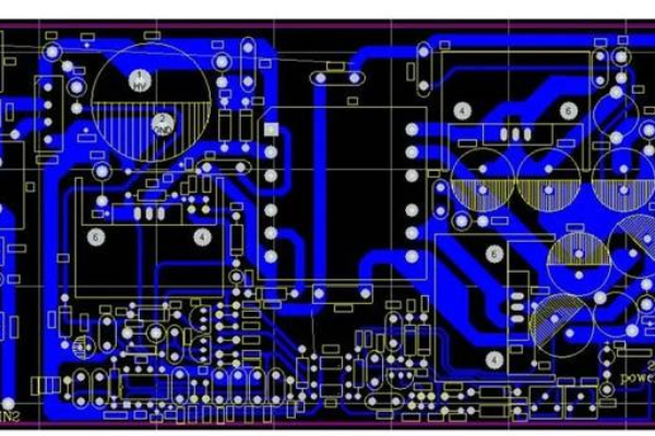
In printed circuit board manufacturing, lamination refers to the process of fusing multiple conductive and insulating layers into a single, cohesive multilayer board through the application of heat and pressure. The standard lamination stack-up consists of several essential components:
•Inner layer cores: Thin PCB substrates with pre-etched copper circuits
•Prepreg layers: Partially cured epoxy resin-impregnated glass fiber sheets that flow during lamination to bond layers together
•Copper foils: Outer conductive layers that form the external circuits after patterning
•Release films: Specialized materials that prevent resin from adhering to press plates
•Buffer materials: Typically Kraft paper used as a thermal buffer between the hot plates and circuit materials
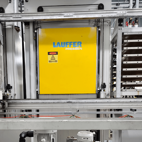
The process occurs in specialized hydraulic or vacuum lamination presses equipped with heated platens that deliver precisely controlled temperature and pressure profiles throughout the curing cycle. These sophisticated manufacturing systems can accommodate multiple press openings simultaneously, each containing several panel stacks to maximize production efficiency.
The Science Behind Lamination
At a molecular level, PCB lamination relies on the complex thermosetting behavior of epoxy resins in the prepreg material. During the heating phase, these resins undergo viscosity reduction, flowing to encapsulate circuit features and eliminate air pockets between layers. As temperature maintenance continues, cross-linking polymerization occurs, transforming the viscous resin into a durable, infusible solid that permanently bonds the layers together.
The Z-direction expansion properties of the resulting composite material must be carefully managed to ensure reliability during subsequent assembly processes and field operation. This dimensional stability is particularly crucial for boards containing plated through-holes, which must maintain electrical continuity despite thermal cycling stresses encountered throughout the product lifecycle.
2.PCB Lamination Process: Step-by-Step
1. Material Preparation and Lay-Up
The lamination process begins with meticulous material preparation in controlled environments:
•Inner Layer Treatment: Copper oxide coating or alternative surface treatments are applied to enhance bond strength between copper surfaces and prepreg materials
•Prepreg Cutting: Glass-fiber reinforced epoxy prepreg sheets are precisely cut to panel dimensions, with careful attention to moisture protection as these materials are hygroscopic
•Lay-Up Sequence: Operators methodically stack materials in the prescribed sequence: release film, copper foil, prepreg, inner layer core, prepreg, copper foil, release film
•Stack Alignment: In traditional lamination, alignment pins maintain registration between layers; in mass lamination, alternative methods preserve layer-to-layer positioning
This preparatory phase typically occurs in cleanroom environments with controlled temperature and humidity to prevent contamination and material degradation prior to pressing.
2. Lamination Cycle Parameters
The actual lamination process follows a carefully orchestrated temperature and pressure profile:
Table: Standard Lamination Cycle Parameters
| Process Stage | Temperature Range | Pressure Range | Key Objectives |
| Kiss Pressure | Room temperature to resin melt point | 15-50 PSI | Allow resin flow while preventing excessive movement |
| Full Pressure | Curing temperature (typically 175°C+) | 300-500 PSI | Complete layer bonding and resin curing |
| Curing | Maintain at 175°C±5°C | Maintain full pressure | Achieve complete resin polymerization |
| Cool-Down | Gradual reduction to safe handling temperature | Maintain pressure until ~50°C | Prevent stress-induced warpage and delamination |
The complete lamination cycle, including heating, curing, and controlled cooling, typically requires 4+ hours to ensure proper resin polymerization and dimensional stability. Thicker boards and those with high copper content often require extended cycle times to achieve complete curing throughout the cross-section.
3. Post-Lamination Processing
After successful lamination, panels undergo several critical processing steps:
•Tooling hole registration: Reference holes are drilled for subsequent processes
•X-ray targeting: Reference points are established for layer-to-layer alignment
•CNC drilling: Creates through-holes for interlayer connections
•Deburring: Removes drilling debris from hole entrances
•Desmearing: Eliminates resin residues from drilled holes
•Electroless copper deposition: Establishes conductive base for subsequent electroplating
Each of these steps prepares the laminated panel for successful formation of electrical interconnections between layers.
3.Critical Lamination Methods and Technologies
Conventional vs. Mass Lamination
The PCB industry has developed two primary lamination approaches:
Traditional Cap Lamination
– Utilizes single-sided copper-clad cores for outer layers
– Each press opening typically contains only one production panel
– Requires precise alignment using tooling pins
– Suitable for low-volume production and prototype applications
Mass Lamination (Mass Lam)
– Employs copper foil for outer layers instead of pre-clad cores
– Multiple panel arrays are laminated simultaneously in each press opening
– Incorporates post-lamination registration systems
– Significantly improves production efficiency for high-volume manufacturing
Specialized Lamination Techniques
Vacuum Lamination
Vacuum-assisted lamination processes have become increasingly important for advanced multilayer boards, particularly those featuring high-density interconnects (HDI) and blind/buried via structures. By removing air from the lamination stack before applying pressure, this method significantly reduces the risk of entrapped gases that can lead to voids or delamination in the finished product.
Autoclave Lamination
Also known as “pressure cooker” processes, autoclave lamination subjects assembled panels to controlled high-pressure steam environments to evaluate delamination resistance and ensure material compatibility with subsequent assembly processes. This method is particularly valuable for qualifying boards intended for harsh operating environments or high-reliability applications.
4.Materials in PCB Lamination
Prepreg (B-Stage) Materials
Prepreg – short for “pre-impregnated” – represents the bonding material that fuses layers together during lamination. These partially cured epoxy resin sheets reinforced with glass fiber cloth are characterized by several critical parameters:
•Resin Content: Percentage of resin by weight, affecting flow characteristics and final dielectric properties
•Gel Time: Duration resin remains fluid at elevated temperature before cross-linking
•Flow Percentage: Degree of resin movement during lamination, critical for filling circuit features
•Volatile Content: Moisture and other vapors that must be eliminated during lamination
Different prepreg classifications offer varying properties to address specific design requirements, with standard FR-4 formulations serving most conventional applications, while specialized materials with modified dielectric properties or thermal performance target high-frequency or high-reliability applications.
Copper Foils
The lamination process incorporates copper foils in various weights and treatments:
•Electrodeposited Copper: Standard material with characteristic columnar grain structure
•Rolled-Annealed Copper: Superior flexibility for dynamic flex applications
•Reverse-Treated Foils: Specialized surfaces for enhanced bond strength
•Low-Profile Foils: Smoother surfaces for high-frequency signal integrity
Copper weights typically range from 1/4 oz (9 μm) to 2 oz (70 μm), with thicker copper requiring adjustments to lamination parameters to accommodate reduced resin flow areas.
Specialized Materials
Advanced PCB designs increasingly incorporate specialized materials to address specific performance requirements:
•High-Tg FR-4: Enhanced thermal resistance for lead-free assembly processes
•Halogen-Free Materials: Environmentally compliant formulations with reduced bromine and chlorine content
•Low-Loss Materials: Specialized resins for high-speed digital and RF applications
•High-CTI Materials: Improved tracking resistance for high-voltage applications

5.Common Lamination Defects and Solutions
Even with sophisticated equipment and controls, lamination processes can produce various defects that impact quality and yield:
Table: Common PCB Lamination Defects and Corrective Actions
| Defect Type | Root Causes | Preventive Measures |
| Voids & Delamination | Insufficient resin flow, entrapped moisture/volatiles, contamination | Implement proper material storage, extend kiss cycle, optimize temperature ramp rate |
| Resin Starvation | Excessive resin flow, inadequate prepreg selection, high copper density | Adjust resin content, optimize pressure profile, incorporate dummy copper features |
| Layer Misregistration | Material instability, tooling inaccuracy, excessive resin flow | Improve dimensional stability, optimize lamination parameters, upgrade tooling systems |
| Warpage & Twist | Asymmetric stack-up, uneven thermal expansion, premature pressure release | Balance copper distribution, implement symmetrical construction, optimize cool-down cycle |
| Copper Wrinkling | Rapid heating, inadequate tensioning, CTE mismatch | Reduce heating rate, improve handling procedures, select compatible materials |
| White Spots | Localized delamination, resin fracture, thermal stress | Optimize lamination profile, improve material compatibility, reduce thermal shock |
Advanced Automated Optical Inspection (AOI) systems, impedance testing, and microsection analysis represent essential quality verification methods for identifying and quantifying these lamination-related defects.
6.Advanced Lamination Applications
HDI and Microvia Technology
High-Density Interconnect structures present unique lamination challenges, particularly when incorporating sequential build-up methodologies. These advanced constructions require:
•Multiple lamination cycles (3-6+ successive laminations)
•Ultra-thin dielectric layers with precise thickness control
•Specialized low-flow or no-flow prepregs to preserve laser via geometry
•Advanced registration systems to maintain layer-to-layer alignment
The transition to any-layer HDI architectures, where microvias can connect any two adjacent layers in the stack-up, demands exceptional process control throughout successive lamination operations.
Heavy Copper and Thermal Management Boards
PCBs designed for high-power applications incorporate substantial copper thicknesses (3-20 oz) that create significant challenges for conventional lamination processes. Successful lamination of these structures requires:
•Extended kiss cycles to accommodate massive copper features
•Specialized high-resin-content prepregs to fill extreme topography
•Modified pressure profiles to prevent resin starvation
•Thermal management materials with enhanced thermal conductivity
These applications often incorporate metal cores or thermal pyramids to dissipate heat, further complicating the lamination process.
RF and Microwave Circuits
High-frequency circuit materials present particular lamination difficulties due to their specialized dielectric properties and often non-standard construction:
•PTFE-based materials with low dielectric constant and loss tangent
•Ceramic-filled substrates with controlled dielectric properties
•Adhesive systems compatible with low-loss materials
•Hybrid constructions combining different material types
Successful lamination of these advanced materials often requires specialized process development to address unique flow characteristics and curing behaviors.
7.The Future of PCB Lamination Technology
The PCB lamination landscape continues evolving to address emerging requirements from next-generation electronic applications:
Industry 4.0 and Smart Manufacturing
Modern lamination facilities are increasingly incorporating Industry 4.0 principles, including:
•Real-time process monitoring with comprehensive data acquisition
•Predictive maintenance algorithms for press equipment
•Adaptive process control based on material lot variations
•Digital twin technology for process optimization
These advanced manufacturing approaches enable tighter process control, improved yield, and reduced operational costs.
Emerging Material Technologies
Several emerging material technologies promise to transform PCB lamination processes:
•Low-Temperature Laminating Materials: Enabling integration of heat-sensitive components
•Ultra-Low Loss Materials: Supporting millimeter-wave applications beyond 5G
•Sustainable Material Systems: Addressing environmental concerns through bio-based resins and recyclable reinforcements
•Embedded Component Technologies: Allowing integration of passive and active components within the PCB structure
Conclusion: Optimizing PCB Lamination for Quality and Reliability
PCB lamination represents far more than a simple bonding process—it is a sophisticated manufacturing discipline that directly determines the performance, reliability, and manufacturability of multilayer circuit boards. As layer counts continue increasing and feature sizes progressively shrink, the importance of precise lamination process control becomes increasingly critical.
Successful lamination requires careful attention to numerous interdependent factors:
•Material Compatibility: Ensuring all stack-up components exhibit compatible thermal and mechanical properties
•Process Optimization: Developing temperature and pressure profiles matched to specific material combinations and board designs
•Quality Verification: Implementing comprehensive inspection methodologies to identify and address defects
•Continuous Improvement: Incorporating data-driven analysis to refine processes and address emerging challenges
For PCB manufacturers, developing expertise in lamination technology represents a significant competitive advantage, particularly as product requirements continue advancing toward higher densities, faster signals, and more demanding operating environments. By mastering the principles and practices outlined in this guide, manufacturers can position themselves at the forefront of PCB technology, delivering innovative solutions that meet the evolving needs of the electronics industry.