Surface-Mount Technology (SMT) has revolutionized the world of PCB assembly (PCBA) by offering faster, more efficient, and cost-effective solutions for placing electronic components onto printed circuit boards. SMT is the standard method used in modern electronics manufacturing, replacing traditional through-hole technology (THT) in most applications. The SMT placement process is crucial to ensuring that the components are placed correctly and securely, with high precision and minimal defects. In this blog, we will explore the different SMT placement processing solutions and their significance in PCB assembly.
Table of Contents
1. What is SMT surface mount technology?
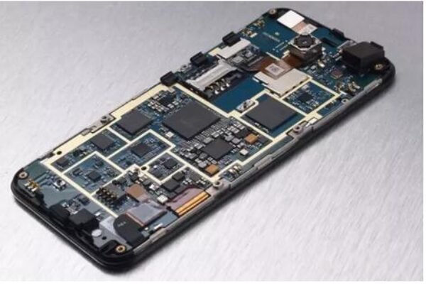
SMT placement refers to the process of positioning electronic components, such as resistors, capacitors, and integrated circuits (ICs), on the surface of the PCB before soldering. The process typically involves the use of automated machines that place the components accurately in a precise pattern, based on the design of the PCB. SMT placement is critical to the overall performance and reliability of the final product, as improper placement can lead to issues such as poor electrical connections, short circuits, and component damage.
2. What are the key technologies for SMT surface mounting?
There are several key technologies involved in SMT placement processing, each offering different benefits in terms of speed, accuracy, and flexibility. Some of the most commonly used SMT placement solutions include:
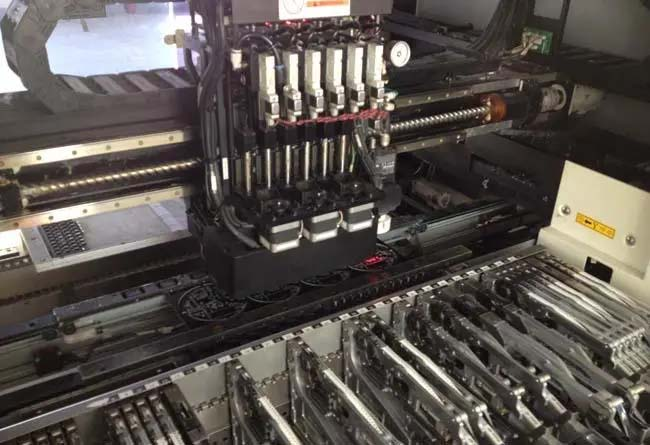
a. Pick-and-Place Machines
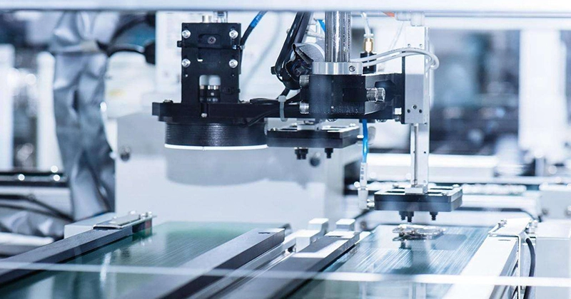
Pick-and-place machines are the heart of the SMT placement process. These machines are designed to automatically pick up components from a feeder and place them on the PCB. They use robotic arms, vacuum nozzles, and advanced vision systems to ensure precise placement. High-end pick-and-place machines can place thousands of components per hour, offering a fast and efficient solution for large-scale production. These machines also incorporate automatic alignment and inspection features to ensure that components are placed accurately according to the PCB design.
b. Manual Placement
While automated systems dominate most SMT processes, manual placement may still be used in low-volume production or for particularly large or complex components that require more precision. Skilled technicians manually place each component on the PCB, ensuring the placement is accurate. Manual placement can be time-consuming and less efficient than automated systems, but it can be necessary for certain specialized applications or for prototypes where a fully automated system may not be justified.
c. Laser or Vision-Guided Placement Systems
Some advanced SMT placement systems use laser or vision-guided technologies for enhanced accuracy and precision. These systems employ high-resolution cameras and lasers to check the position of components in real time, making fine adjustments during placement. This improves the accuracy of component positioning, especially for smaller or more complex components, such as fine-pitch ICs. Vision-guided systems are particularly beneficial when dealing with smaller boards or higher component density, where precise alignment is critical.
3. Challenges in SMT Placement Processing
Despite its advantages, SMT placement processing comes with several challenges that need to be addressed to ensure a high-quality PCBA. Some of the key challenges include:
a. Component Misalignment
Misalignment during placement can lead to issues such as soldering defects, poor electrical contact, and short circuits. This is particularly a concern when placing components with fine-pitch leads or small sizes. The use of advanced placement machines with vision systems and proper calibration can help mitigate this problem.
b. Component Handling
Components used in SMT are often very small and delicate, requiring precise handling to avoid damage. If components are mishandled or subjected to excessive force, it can result in broken or bent leads, compromising the integrity of the PCBA. Proper component handling and storage solutions, such as vacuum-based handling systems, are necessary to prevent such issues.
c. Placement Speed vs. Accuracy
In high-volume production, there is often a trade-off between placement speed and placement accuracy. While faster placement is desirable for throughput, it can sometimes compromise precision, especially when dealing with small or complex components. Finding the right balance between speed and accuracy is essential for maintaining product quality while meeting production deadlines.
4. Automated Optical Inspection (AOI) and Inline Testing
To further ensure the quality of the SMT placement process, Automated Optical Inspection (AOI) systems are often employed. These systems use cameras to inspect the PCB after the placement process to detect any misalignments, missing components, or soldering defects. AOI systems are highly effective in detecting placement errors early in the production process, reducing the chances of defects reaching later stages such as soldering.
Additionally, inline testing such as in-circuit testing (ICT) and functional testing can be used to validate the correct placement of components. ICT tests the electrical connections of each component, while functional tests verify the PCB’s overall performance.
5. Innovative Trends in SMT Placement Processing
As technology continues to advance, there are several innovative trends in SMT placement processing that are reshaping the industry:
a. Machine Learning and AI in SMT Placement
Artificial intelligence (AI) and machine learning algorithms are being integrated into SMT placement machines to improve process efficiency and reduce defects. These systems can learn from previous production data, optimize placement patterns, and even predict potential issues, allowing for proactive adjustments.
b. Industry 4.0 Integration
Industry 4.0 principles are increasingly being applied to SMT placement. With real-time monitoring, data analytics, and machine connectivity, manufacturers can gain deeper insights into the performance of SMT placement systems and make adjustments dynamically to optimize production.
c. Miniaturization of Components
As electronic devices continue to get smaller and more complex, the trend toward miniaturization of components has put pressure on SMT placement systems to handle smaller, more intricate parts. Advances in pick-and-place technology are addressing this challenge, with new machines capable of placing components with pitch sizes as small as 0.3mm.
6. Conclusion
SMT placement processing is a crucial step in the PCB assembly process, directly affecting the performance, reliability, and cost-effectiveness of the final product. Whether through automated pick-and-place machines, manual placement, or advanced vision-guided systems, manufacturers must choose the right placement solution to meet the demands of their specific applications. Overcoming the challenges of alignment, handling, and balancing speed with accuracy is essential for achieving high-quality PCBs. As the industry evolves, the integration of AI, machine learning, and Industry 4.0 technologies promises to further enhance the capabilities and efficiency of SMT placement processing, enabling even higher precision and faster production cycles.