As the core carrier of communication equipment, Phone PCB play a crucial role in fixed line telephones, VoIP devices, wireless telephones, and other scenarios. With the evolution of communication technology from analog to digital, the design of PCB needs to balance voice signal fidelity, anti-interference capability, and cost-effectiveness. This article deeply analyzes the technical points and industry trends of telephone PCB from design specifications, signal integrity assurance to manufacturing processes.
—
Table of Contents
1、 Core application scenarios of Phone PCB Design
1. Fixed phone system
The traditional landline circuit board needs to support dual tone multi frequency (DTMF) signal analysis and speech signal amplification, and the design needs to focus on optimizing the anti noise performance of the analog circuit module.
2. VoIP (Voice over Internet Protocol) devices
Integrating Ethernet PHY chips with speech codecs (such as G.711/G.729) requires a four layer stacked structure (such as TOP-GND Signal PWR) to reduce the interference of digital signals on analog speech.
3. Wireless phone and DECT System
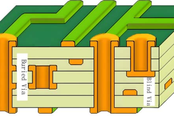
The high-frequency module (1.8GHz-2.4GHz) needs to be designed with microstrip lines and ceramic filters, using blind buried hole technology to shorten the RF path and control the insertion loss within 0.5dB.

—
2、 Design points and signal integrity optimization
1. Hierarchical architecture and impedance control
-Recommended structure for four layer board: The signal layer is adjacent to the complete ground plane, with an impedance tolerance of ± 10% (single end 50 Ω, differential 100 Ω), to avoid signal reflection caused by cross segmented wiring.
-Analog/digital partitioning: By dividing the ground plane and isolating it with magnetic beads, it reduces mixed digital and analog noise (such as ADC module signal-to-noise ratio needs to be ≥ 70dB).
2. Power and noise management
-Adopting a star shaped grounding topology, a 10 μ F electrolytic capacitor is arranged at the main power inlet, and a 0.1 μ F ceramic capacitor is placed next to the chip power pin to form the shortest circuit of “power capacitor ground”.
-The high current path (such as ringing circuit) uses 2oz thick copper, combined with a heat dissipation via array (≥ 8/cm ²), reducing temperature rise by 30%.
3. High frequency signal processing
-The RF wiring adopts a strip line structure with ground planes on both sides, and the line width is accurately calculated based on the dielectric constant (such as Dk=4.5 for FR-4).
-Differential pairs (such as USB interfaces) are strictly equal in length (with an error of ± 0.1mm), and the spacing between serpentine lines is ≥ 3 times the line width to reduce common mode noise.

—
3、 Manufacturing process and reliability assurance
1. Application of HDI technology
For miniaturized devices such as cordless phones, laser drilling (aperture ≤ 0.15mm) and stacking technology are used to increase wiring density by 40%. At the same time, thermal stress distribution is verified through simulation (error ≤ 2 ℃).
2. DFM compatibility design
-Line width/spacing ≥ 6mil, through-hole inner diameter ≥ 8mil, suitable for most board factory processes;
-Avoid sharp angle wiring and use 45 ° or rounded corners to reduce impedance transients and EMI radiation.
3. Testing and Verification Process
-Functional testing: Verify the DTMF decoding accuracy (target ≥ 99.9%) and speech frequency response (300Hz-3.4kHz ± 1dB) through the ATS system.
-Environmental testing: Conduct 1000 temperature cycling tests at -40 ℃~85 ℃ to ensure that the porosity of solder joints is less than 15%.
—
4、 Industry Trends and Innovative Technologies
1. IoT integration
The new generation IP phone circuit board integrates Wi Fi/Bluetooth modules and adopts a six layer board mixed voltage design (RO4350B+FR4), supporting PoE power supply and voice data encryption.
2. Hardware based AI noise reduction algorithm
Real time echo cancellation (AEC) and background noise suppression are achieved through FPGA, with a computation delay of less than 10ms, and power supply integrity needs to be optimized (ripple ≤ 50mV).
—
Reference source: Industry technical standards and practical data, some cases refer to communication equipment design guidelines.