Driven by high-speed communication, new energy vehicles, and intelligent hardware, the selection and design of diodes in PCBs directly affect circuit stability and energy efficiency. This article comprehensively analyzes the key technical points of diodes in PCB from core functions, selection parameters, layout specifications to industry applications, helping enterprises improve design reliability.
—
Table of Contents
1、 Core functions and common types of diodes
1. Current control and protection
Diodes achieve rectification, voltage clamping, and anti reverse protection through unidirectional conductivity. For example, Schottky diodes (VF as low as 0.3V) can reduce power losses, while TVS diodes (such as SMAJ series) can suppress 10kV surge voltage and protect sensitive ICs.
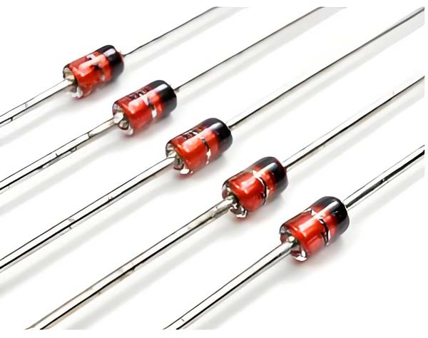
2. Mainstream diode types and applicable scenarios
-Rectifier diode (1N4007): used for AC/DC conversion, with a current carrying capacity of 1A;
-Zener diode (BZX85): voltage stabilization accuracy ± 5%, suitable for voltage reference circuits;
-TVS diode (SMAJ5.0A): response time<1ps, used for ESD protection;
-Schottky diode (BAT54S): In high-frequency switching scenarios, the reverse recovery time is only 4ns.

—
2、 Key parameters for PCB diode selection
1. Electrical performance indicators
-Forward voltage (VF): Low VF (such as 0.3V) can reduce power consumption and is suitable for portable devices;
-Reverse recovery time (Trr): High frequency scenarios require Trr<4ns (such as BAV99);
-Thermal resistance (R θ JA): It is recommended that the power consumption under SOT-23 packaging should not exceed 50% of the rated value.
2. Environmental adaptability parameters
-Junction temperature (Tj): Vehicle grade components must meet the working range of -40 ℃~150 ℃ (AEC-Q101 certification);
-Packaging compatibility: Micro SMT packaging (such as DFN1006) saves space, but requires optimized heat dissipation paths.
—
3、 Diode Layout and EMC Optimization Strategy
1. The Golden Rule for TVS diode layout
-Near end protection: TVS should be located adjacent to the I/O interface (spacing ≤ 5mm) to reduce surge path inductance;
-Grounding treatment: Surge current should be directed towards the chassis ground rather than the signal ground, and the grounding line width should be ≥ 2mm to reduce impedance.
2. Parasitic parameter control in high-frequency scenarios
-Adopting a short lead layout to reduce parasitic inductance (increasing inductance by approximately 1nH per 1mm wire);
-Sensitive signal lines (such as clock lines) adopt a grounded design, with ground hole arrays arranged on both sides.
—
4、 Manufacturing Process and Reliability Design
1. Thermal management scheme for SMT packaging
-The copper foil area of the solder pad is ≥ 1.5 times the size of the device, and it is connected to the inner ground plane through a through-hole for heat dissipation;
-Use thermal simulation tools (such as ANSYS Icepak) to predict the junction temperature and ensure that the temperature rise is ≤ 15 ℃.
2. Welding process optimization
-The reflow soldering temperature curve needs to match the packaging size (such as SOD-323 peak temperature ≤ 245 ℃);
-Use X-ray to detect the porosity of solder joints, ensuring that the porosity is less than 15%.
—
5、 Analysis of Industry Application Cases
1. BMS system for new energy vehicles
-Adopting AEC-Q101 certified TVS diodes (such as SMBJ30CA) to protect against transient voltage of 12V battery pack;
-Copper substrate+thermal conductive adhesive design reduces temperature rise by 40%.
2. 5G base station RF module
-High frequency Schottky diode (HSMS-286x) achieves 28GHz signal rectification with insertion loss<0.5dB;
-The mixed pressure PCB structure (RO4350B+FR4) balances cost and performance.
—
If you need customized solutions, please feel free to contact our engineering team!
Reference source: Industry technical standards and practical data.