Table of Contents
The GPU PCB Landscape: Where Performance Meets Precision
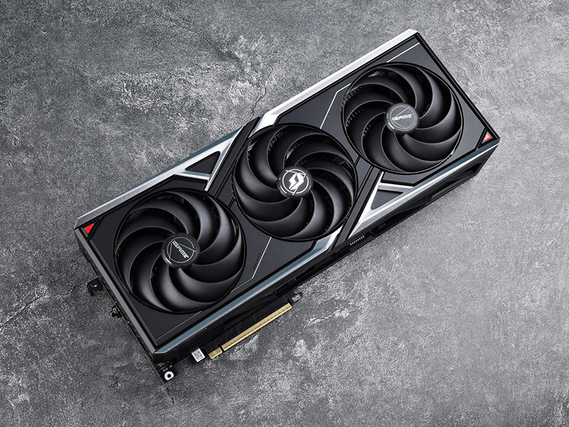
As AI training clusters expand and gaming GPUs push teraflop boundaries, one critical enabler remains hidden in plain sight: the printed circuit board. GPU PCBs have evolved from simple interconnect platforms into sophisticated electro-mechanical systems that balance signal integrity, thermal dynamics, and power delivery at unprecedented scales. With global AI PCB demand projected to reach ¥69.3 billion by 2026—driven largely by GPU accelerators—these substrates now dictate performance ceilings more than ever.
Breaking Density Barriers: Cutting-Edge Layout Strategies
1. 3D Stacked Memory Architecture
Space-constrained designs (like laptops or compact accelerators) now leverage clamshell stacking—mounting identical memory modules on both sides of the PCB directly opposite each other. This technique:
– Halves footprint: A 4-memory setup occupies the board area of just two modules
– Simplifies routing: Shared vias connect paired modules, reducing layer count
– Maintains signal timing: Symmetric paths preserve critical clock synchronization
In NVIDIA-inspired layouts, GPU-centric quadrant zoning places memories within strict geometric boundaries (e.g., 150–200 mil from GPU vertices), enabling clean 6-layer designs where 8 layers were previously mandatory.
2. Orthogonal Backplanes: Replacing Copper Cables
The AI infrastructure shift from bulky cable jungles to PCB orthogonal backplanes marks a watershed moment. NVIDIA’s Rubin Ultra NVL576 racks will likely pioneer this with:
– 70+ layer boards: Incorporating ultra-low-loss M9-grade laminates
– Direct GPU-NVSwitch routing: Enabling terabyte-scale interconnects in constrained spaces
– Thermal resilience: Copper planes dissipate heat more effectively than bundled cables
> Single-rack PCB values could reach ¥800K–¥1M, potentially adding ¥20B to the PCB market by 2027.
Critical Design Enablers for High-Performance GPU PCBs
Layer Stackup Optimization
| Layer Count | Typical GPU Class | Key Characteristics |
| 6 layers | Mid-range gaming | Cost-effective; supports GDDR6 < 18Gbps |
| 8 layers | Flagship gaming | Enables stable 550–650MHz memory overclocks |
| 10–12 layers | Workstation/AI | Critical for 112G PAM4 signaling (e.g., NVLink) |
| 70+ layers | AI rack backplanes | Orthogonal GPU-switch interconnects |
Data synthesized from
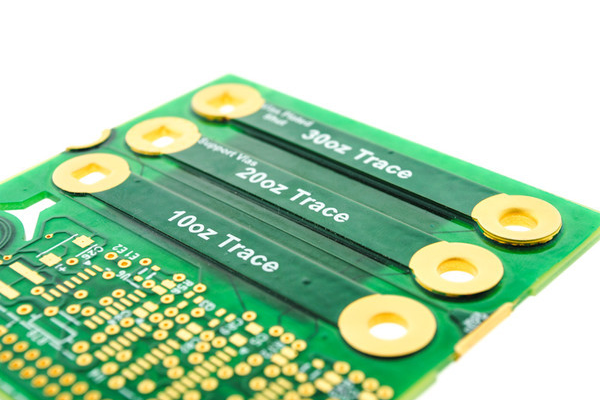
Higher layers reduce crosstalk but exponentially increase cost. Strategic impedance-controlled striplines (traces routed between ground planes) in 8-layer designs can match 10-layer performance for many applications.
Laser-Drilled Microvias: Non-Negotiable for HDI
- AI GPU substrates: 100% of core vias require laser drilling for <100µm precision
- Mechanical drills: Limited to peripheral holes due to positional tolerance >50µm
- Benefits: Tighter registration enables 20% higher trace density versus mechanical drilling
Laser systems now dominate 80% of the HDI microvia market—a prerequisite for next-gen AI accelerators.
Emerging Technologies Reshaping GPU PCB
CoWoP Packaging: Eliminating the Substrate
NVIDIA’s exploration of Chip-on-Wafer-on-PCB (CoWoP) signals a radical departure:
– Direct die-to-PCB bonding: Removes traditional organic substrates
– 15% signal integrity gain: By eliminating substrate dielectric losses
– Enhanced thermal management: Cold plates contact silicon directly (no lid)
– Targeted adoption: Rubin GR150 GPUs (2027 production)
While CoWoP promises revolutionary benefits, its complexity may prolong CoWoS’s dominance for mainstream GPUs through 2028.
Server-Optimized Form Factors
Chinese AI hardware innovators demonstrate how retail GeForce PCBs are re-engineered into data center accelerators by:
– Re-layout into 2-slot profiles: Replacing triple-fans with blower coolers
– Edge-shifted power connectors: Preventing cable interference in dense racks
– Robotic rework systems: Transplanting GDDR7/GDDR7X modules onto server-grade PCBs
Thermal and Power Integrity: The Silent Performance Limiters
Copper balancing isn’t optional—asymmetrical copper distribution causes warping during reflow soldering. Modern GPU PCBs combat this via:
– 20–30% copper-filled planes: In critical power delivery zones
– Arrayed thermal vias: Under GPU packages (often solder-filled for 15–30% better heat transfer)
– Decoupling capacitor pyramids: 0201/01005-size MLCCs within 1.5mm of BGA pads
Power integrity simulations (HyperLynx, Sigrity) are now mandatory to validate sub-2% voltage ripple under 2,000A GPU transient loads.
Conclusion: Partnering for the GPU Acceleration Era
From laser-drilled HDI microvias to orthogonal backplanes, GPU PCBs have become precision instruments where every micrometer influences teraflops. As AI clusters demand 70+ layer substrates and CoWoP packaging looms, only PCB partners with proven expertise in impedance control, thermal management, and ultra-HDI can deliver reliable solutions.
Get your exclusive quote immediately: fill out the form or send an email directly.As a professional PCB manufacturer for hobbyist , we will provide you with a quote service within 24 hours. Enjoy free DFM optimization and a 10% discount on SMT patches for your first order!