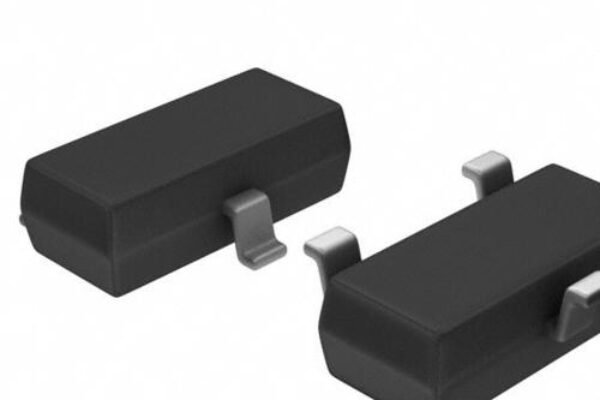
Load switch IC have evolved from simple power gates into sophisticated power management solutions that directly impact system efficiency, reliability, and form factor. These compact devices sit between a power source and load, providing critical functions like inrush current control, reverse current blocking, and intelligent power sequencing—features once achievable only through complex discrete circuits. For PCB designers, mastering load switch implementation is now essential for next-generation electronics.
Table of Contents
Core Functions & Technical Advantages
1.Intelligent Power Switching
- Active Current Limiting: Devices like Nexperia’s NPS4053 enable programmable current limits (110mA–2.5A, ±6% accuracy), preventing circuit damage during faults .
- Soft-Start Control: Integrated slew rate management (e.g., Kinetic KTS1601) minimizes inrush current, reducing voltage droops and EMI in sensitive analog circuits .
- True Reverse Current Blocking (TRCB): Littelfuse’s LQ05041RCS6 eliminates backflow without external diodes—critical for battery-operated devices .

- Active Current Limiting: Devices like Nexperia’s NPS4053 enable programmable current limits (110mA–2.5A, ±6% accuracy), preventing circuit damage during faults .
- Soft-Start Control: Integrated slew rate management (e.g., Kinetic KTS1601) minimizes inrush current, reducing voltage droops and EMI in sensitive analog circuits .
2.Ultra-Low Power Operation
Modern load switches optimize battery life through:
- Sub-μA Quiescent Current: Littelfuse ICs achieve industry-low IQ, cutting parasitic drain in wearables/IoT .
- Fast Discharge Paths: Onsemi’s NCP436 includes auto-discharge (8Ω internal) to safely reset loads when disabled .
3.Integrated Protection
- Thermal shutdown, UVLO (Under-Voltage Lockout), and ±8kV ESD hardening (Southchip SC7000) ensure robustness in industrial/automotive environments .
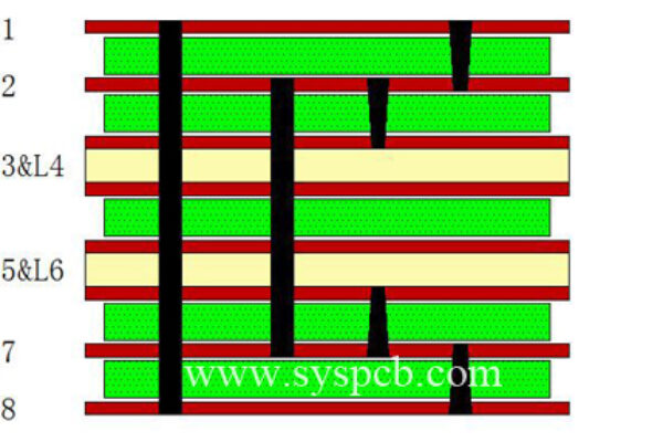
PCB Layout Optimization Strategies
Space-Constrained Designs
- CSP/WLCSP Adoption: Toshiba’s 0.79mm² TCK10XAG and Onsemi’s WLCSP-6 (1.0×1.5mm) enable routing in M.2 SSDs and hearing aids .
- Via-in-Pad Techniques: Essential for thermal management under high-current switches (e.g., 3A+). Fill vias with solder to enhance heat dissipation .
Power Integrity Essentials
- Low Rdson MOSFETs: Southchip SC7000’s 12mΩ Rdson minimizes conduction losses at 5A loads .
- Decoupling Capacitors: Place 0201/01005 MLCCs within 1.5mm of switch inputs to suppress transient noise .
Signal Integrity Preservation
- Separate Analog/Digital Grounds: Isolate switch GND pins from noisy digital returns.
- Guard Rings: Enclose high-impedance enable pins to prevent false triggering.
Key Applications & Load Switch Selection
Table: Load Switch Solutions by Application
| Application | Requirements | Recommended ICs | PCB Impact |
| USB Charging Ports | BC1.2/Apple/Samsung protocols | Southchip SC7000 | 6-layer max; 2oz copper for 5A |
| SSD Power Rails | Sequential power sequencing | Toshiba TCK10XAG + LDO | HDI microvias; ≤4-layer stackup |
| Wearables/IoT | IQ < 2μA; <1mm² footprint | Littelfuse LQ05021 (0.77mm²) | Flexible PCB compatible |
| Automotive IVI | AEC-Q100; 40V tolerance | Nexperia NPS4053 | 6–8 layers; thermal vias array |
Cutting-Edge Innovations
1.Protocol-Integrated Switches
ICs like Southchip SC7000 embed USB PD negotiation, eliminating external microcontroller overhead .
2.Monolithic Integration
Nexperia’s NPS4053 replaces 10+ discrete components (MOSFETs, diodes, comparators), shrinking layouts by 85% .
3.High-Density Power Management
Littelfuse’s multi-bump WLCSPs (0.4mm pitch) support 4A in sub-1mm² areas—ideal for AR glasses .
Why Partner with PCB Experts for Load Switch Integration?
Load switches simplify power architecture but introduce new design challenges:
– Thermal Stress: 3A+ continuous current demands 2oz copper pours and thermal relief patterns.
– Material Selection: High-speed switches (e.g., >100kHz) require ultra-low-loss laminates (Isola FR408HR or Rogers RO4350B).
– DFM Compliance: Microvia fill specifications (conductive vs. non-conductive) vary by vendor and affect reliability .
Your PCB Partner’s Value Proposition:
– Signal Integrity Simulation: Pre-layout analysis for impedance control in 10Gbps+ interfaces.
– HDI Expertise: Laser-drilled microvias (≤75μm) and stacked via builds for chip-scale packages.
– Thermal Modeling: Identify hotspots under high-Rdson switches using CFD tools.
Conclusion: Enabling Smarter Power Domains
Load switch ICs represent the convergence of power efficiency, intelligent control, and integration density. As devices scale from milliwatts (wearables) to kilowatts (AI accelerators), these ICs will continue displacing discrete solutions—making PCB layout precision and manufacturer collaboration non-negotiable.
Get your exclusive quote immediately: fill out the form or send an email directly.As a professional PCB manufacturer for hobbyist , we will provide you with a quote service within 24 hours. Enjoy free DFM optimization and a 10% discount on SMT patches for your first order!