Table of Contents
Introduction: The AI Hardware Revolution Demands PCB Innovation
The launch of GPT-5 marks a quantum leap in AI capabilities, requiring unprecedented computational power and hardware sophistication. As AI models scale exponentially, printed circuit boards (PCBs)—the foundational backbone of electronics—face transformative demands. For PCB manufacturers, this shift presents both challenges and opportunities: high-density interconnects, extreme signal integrity, and thermal resilience are now non-negotiable. By 2029, the global PCB market for AI/data centers alone will surge to $21 billion, driven by AI server deployments and data infrastructure expansion.
1. GPT-5’s Direct Impact: Pushing PCB Technology Boundaries
1.1 Layer Count & Complexity Surge
- AI servers (e.g., NVIDIA DGX systems) now require 28–46-layer PCBs, up from traditional 8–16 layers, to support GPU clusters and high-speed interconnects like PCIe 6.0.
- Value per unit skyrockets: AI server PCBs command 5–7× higher value than conventional boards due to ultra-low-loss materials and microvia stacking.
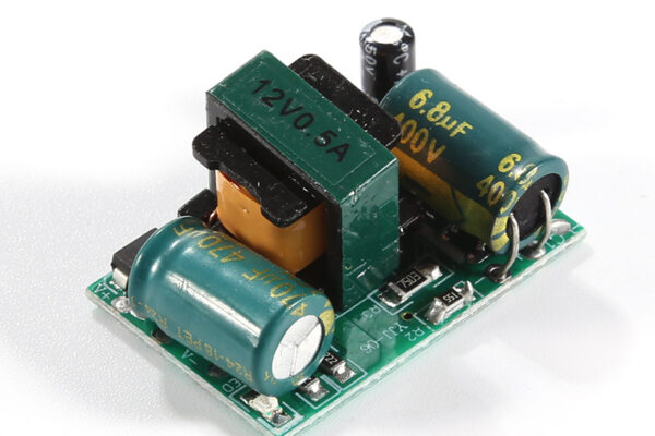
1.2 Material Revolution
- High-frequency substrates: Megtron 6/8 (Panasonic) and hydrocarbon-based laminates replace FR-4 for <0.5 dB/inch signal loss at 56+ Gbps speeds.
- Thermal management: Copper-filled vias, embedded heat spreaders, and ceramic-coated metals dissipate heat from 1000W+ GPUs.
1.3 Precision Manufacturing Challenges
- Aspect ratios >20:1 (e.g., 0.2mm holes in 4mm boards) demand laser drilling and electroplating advancements to avoid voids.
- Impedance tolerance ±3%: Critical for PCIe 6.0 and DDR5 interfaces, requiring AI-optimized dynamic rule engines.
2. AI-Driven Transformation Across the PCB Workflow
2.1 Design & Prototyping: From Weeks to Hours
- Generative AI tools (e.g., Cadence Cerebrus) automate high-speed routing:
- Optimize BGA escape routing for 32+ differential pairs in minutes.
- Predict EMI hotspots with 89% accuracy, slashing respins.
- Cost-performance tradeoffs: AI algorithms recommend hybrid stackups (e.g., FR-4 + high-speed layers), cutting costs by 32% with minimal performance loss.
2.2 Manufacturing Intelligence: Efficiency at Scale
- Automated MI extraction: GPT-powered systems (e.g., Saiet’s Shanmou GPT) parse Gerber/PDF files in minutes (vs. 4–6 hours), achieving 95% parameter accuracy.
- Predictive maintenance: AI vision monitors solder paste quality and via fill integrity, reducing defects by 30%.
2.3 Supply Chain Resilience
- Real-time risk alerts: AI tracks component shortages (e.g., “U5 lead time >20 weeks, switch to ISL85403”).
- Localized production: Southeast Asian hubs (Thailand, Vietnam) emerge as alternatives amid trade tensions.
3. Growth Frontiers: Where PCB Investment Is Concentrated
| Application | Key PCB Requirements | Market Growth (2025–2029) |
| AI Servers | 18+ layers, ultra-low-loss materials | 16.7% CAGR ↗ $25B+ |
| Automotive AI | HDI for lidar, 3–5× higher PCB content | 12.4% CAGR ↗ $18.2B |
| 5G/6G Infrastructure | PTFE-based RF PCBs for mmWave stability | 9.8% CAGR ↗ $14.3B |
4. The Road Ahead: Strategic Shifts for PCB Manufacturers
4.1 Technology Investments
- HDI/microvias: Adopt any-layer HDI and via-in-pad (POFV) for AI chips and wearable miniaturization.
- ABF substrate R&D: Capitalize on chiplet packaging trends; target 50%+ growth in FC-BGA substrates.
4.2 Sustainability Imperatives
- Green manufacturing: Reduce energy consumption by 18% (per China’s 2025 policy) via automation and lead-free solders.
- Recycled materials: Copper foil recovery systems cut costs and comply with EU carbon tariffs.
4.3 Workforce Evolution
- AI-augmented engineers: Shift from manual layout to “AI training” for constraint definition and innovation.
- Upskilling: Cross-train teams in AI tooling (e.g., Ansys HFSS AI modules) and thermal simulation.
Conclusion: Positioning for the AI-Powered PCB Era
GPT-5 is not just a software milestone—it’s a hardware catalyst. The PCB industry must evolve through:
– Material science leadership: Partner with CCL suppliers (e.g., Shengyi Tech) for localizing high-frequency laminates.
– AI/automation integration: Deploy generative design and predictive maintenance to compress lead times.
– Supply chain agility: Diversify产能 into policy-supported regions (e.g., Chinese inland parks or Thailand).
The winners will be those who treat PCBs not as passive carriers, but as active performance enablers for AI.
Why Partner with SysPCB?
As AI hardware demands escalate, we deliver:
– Cutting-edge capabilities: 28+ layer boards, impedance control (±3%), and POFV for via-in-pad designs.
– AI-driven efficiency: GPT-5-ready workflows for rapid prototyping and zero-defect mass production.
– Sustainable scale: IATF 16949-certified plants with 18% lower carbon footprint vs. industry average.
Ready to power the AI revolution? Contact SysPCB for high-reliability PCBs built for GPT-5 and beyond.