Table of Contents
What Is Impedance Control PCB?
The principle of impedance control PCB is mainly to precisely control the impedance of PCB wiring to ensure the stability and integrity of signals during transmission. Impedance is the relative relationship between current and voltage in a circuit, which combines the effects of resistance, inductance, and capacitance, and is typically expressed in ohms (Ω).
Impedance controlled PCBs are commonly used in applications that require high signal integrity, such as high-frequency, radio frequency, or digital signal transmission, such as communication equipment, radio frequency bands, high-speed data transmission, and other fields. Its purpose is to ensure that the signal can be matched with the expected impedance value during transmission on the circuit board, and to minimize signal reflection, crosstalk, and power loss as much as possible.
PCB impedance characteristics and controlled impedance concept principle:
1. Impedance Characteristics

- Impedance is the relative relationship between current and voltage in a circuit. It includes a combination of resistance, inductance, and capacitance, usually represented as a complex number with real and imaginary parts.
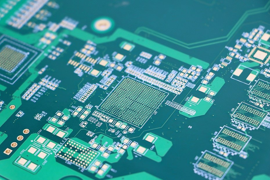
- In PCBA circuit boards, impedance characteristics refer to the resistance, inductance, and capacitance response of signal transmission lines on the circuit board to high-frequency or high-speed signals. The correct matching of impedance characteristics is crucial for ensuring stable signal transmission, especially in differential signals, high-speed buses, and high-frequency applications.
- By precisely controlling the width, spacing, interlayer spacing, material properties, and other parameters of the circuit, the required impedance characteristics can be achieved to ensure accurate signal transmission. This helps reduce signal attenuation, crosstalk, and other circuit issues.
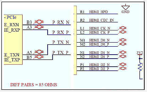
2. Controlled Impedance
- Controlled impedance refers to a specific impedance value that is precisely controlled and maintained on the PCBA circuit board to ensure stable signal transmission. Usually used in high-frequency, high-speed, or differential signal lines.
- For specific applications, design engineers will determine the required impedance values, and then manufacturers must precisely control the parameters of the circuit during the PCB manufacturing process to meet these requirements.
- Controlled impedance typically involves the use of specific circuit design rules, material selection, and manufacturing processes, such as controlling circuit width, spacing, and interlayer spacing, to ensure the desired impedance value.
In high-frequency and high-speed electronic applications, such as communication devices, high-performance computers, RF circuits, etc., the correct implementation of controlled impedance is crucial because it can reduce signal loss, crosstalk, and timing issues, thereby ensuring the reliability and performance of the circuit.
Application of impedance control PCB:
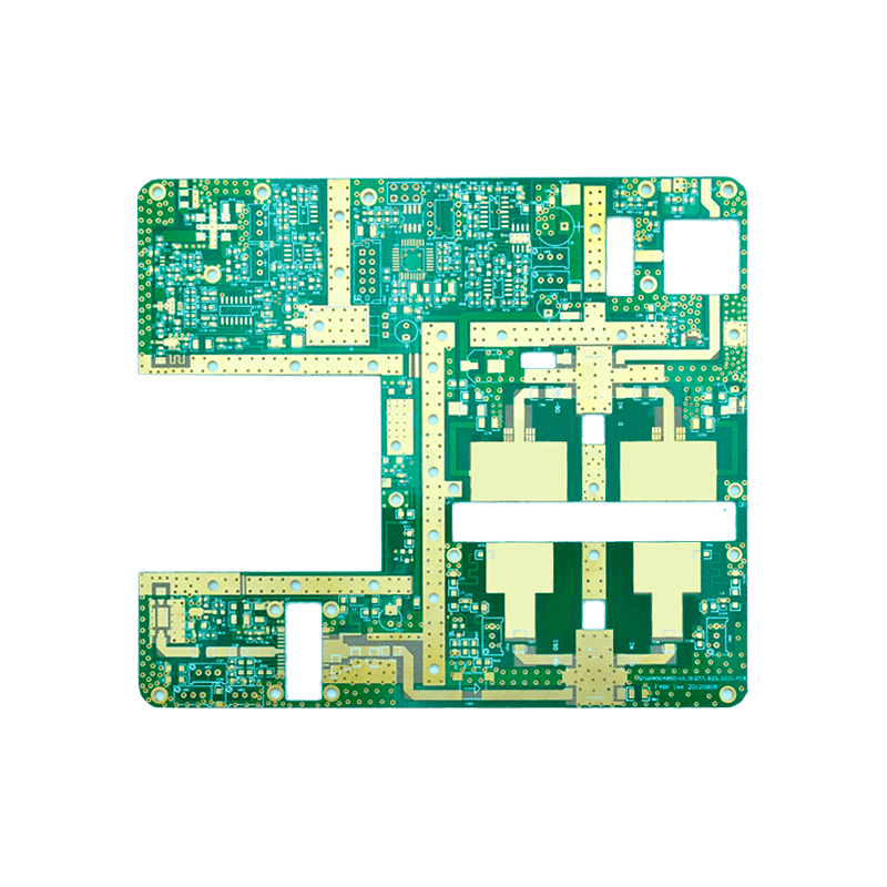
Impedance controlled PCBs are widely used in high-speed circuits, high-frequency circuits, and digital signal processing fields.
For example, impedance control is crucial in applications such as communication devices, high-performance computers, and RF circuits to ensure signal integrity and resistance to noise interference. The design of multi-layer PCB impedance boards provides a high-speed and low interference signal transmission solution by precisely controlling the performance of signal transmission paths.
The specific method of impedance control PCB:
- Optimize circuit layout: By using a reasonable circuit layout and layered wiring method, reduce inter board coupling and signal bounce, and minimize implant distortion.
- Choose suitable materials: Use high-frequency rare earth dielectric isolation plates, high Tg plates, PP plates and other high-frequency materials to improve the stability of signal transmission and reduce transmission losses.
- Adjust line width and spacing: Calculate the most reasonable line width and spacing based on signal frequency and circuit board characteristic parameters to ensure impedance matching.
- Using simulation and design tools: Simulate circuit behavior, signal transmission loss, and electromagnetic interactions through simulation software to determine the optimal PCB design parameters.
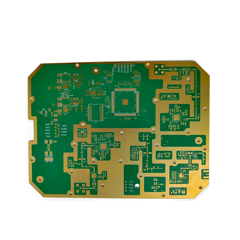
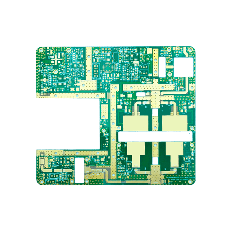
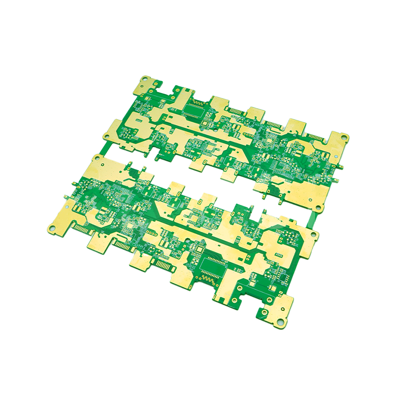
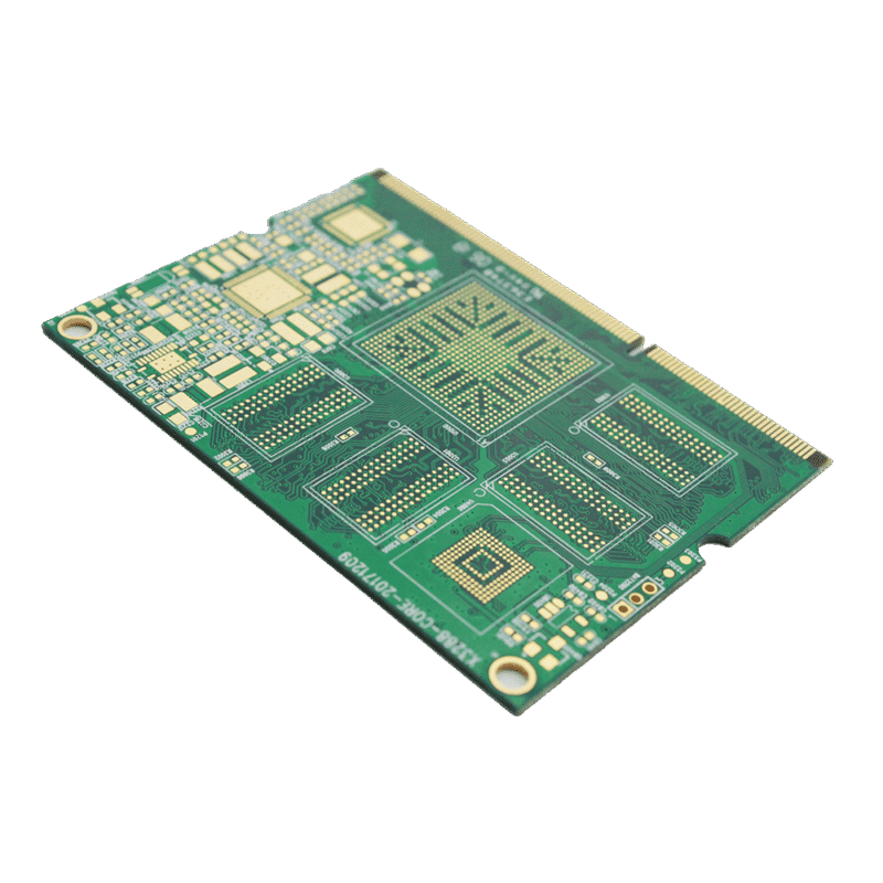
Why choose SysPCB as the supplier for impedance control PCB?
Impedance control PCBs are commonly used in high-frequency PCBs, where each type requires specific impedance values. Since these PCBs are utilized in high-frequency electronic devices, their manufacturing process involves stringent requirements. Selecting a dependable supplier for impedance control PCBs is essential to achieve optimal performance. SysPCB offers several key advantages as a trusted provider of controlled impedance PCBs. Here are some reasons to choose us:
- Extensive Expertise: Over a decade of experience in Impedance control PCB manufacturing.
- Affordable Solutions: Competitive pricing with no minimum order quantity (No MOQ) and flexible, negotiable terms.
- Superior Quality: High-quality assurance backed by professional production facilities.
- Comprehensive Services: End-to-end solutions with a strong focus on customer satisfaction throughout the process.
- Timely Delivery: Fast turnaround times paired with reliable post-sales support.
We can provide personalized professional services to meet your specific impedance control PCB needs. If you have any requirements, please contact us to obtain controllable impedance PCB supply.