Table of Contents
What is IC Substrate PCB?
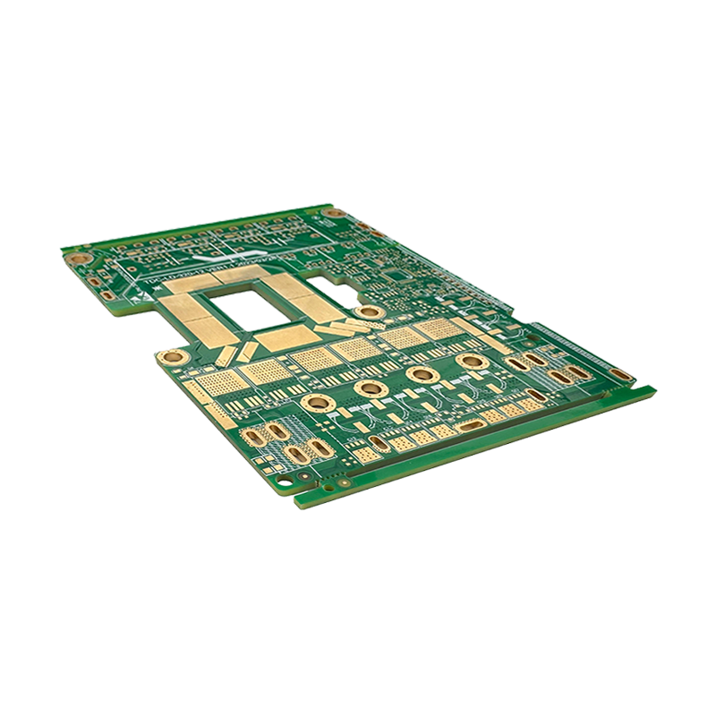
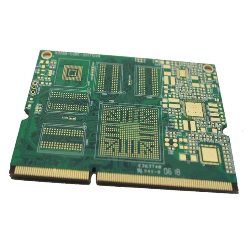
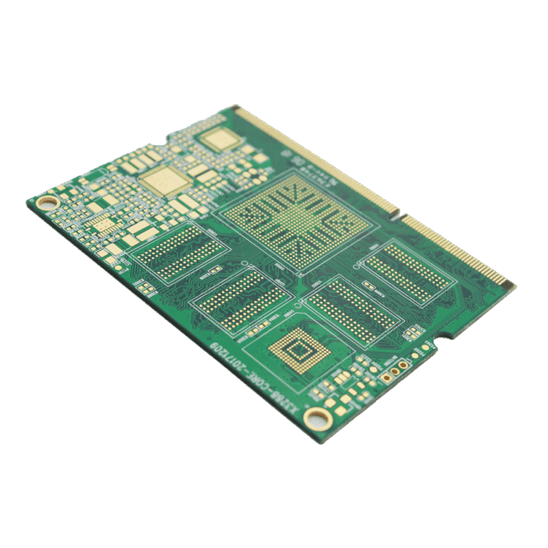
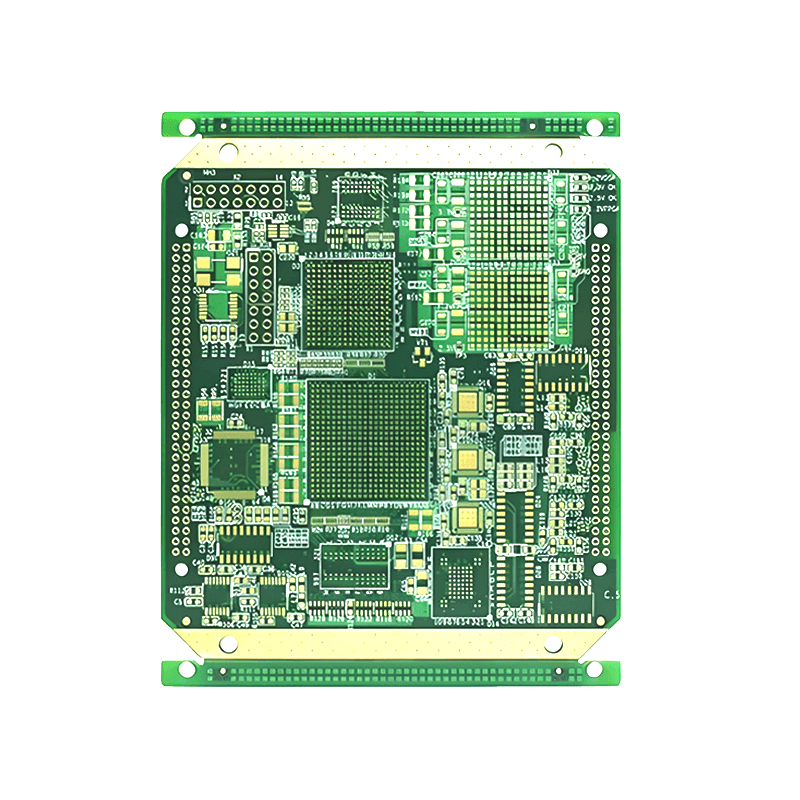
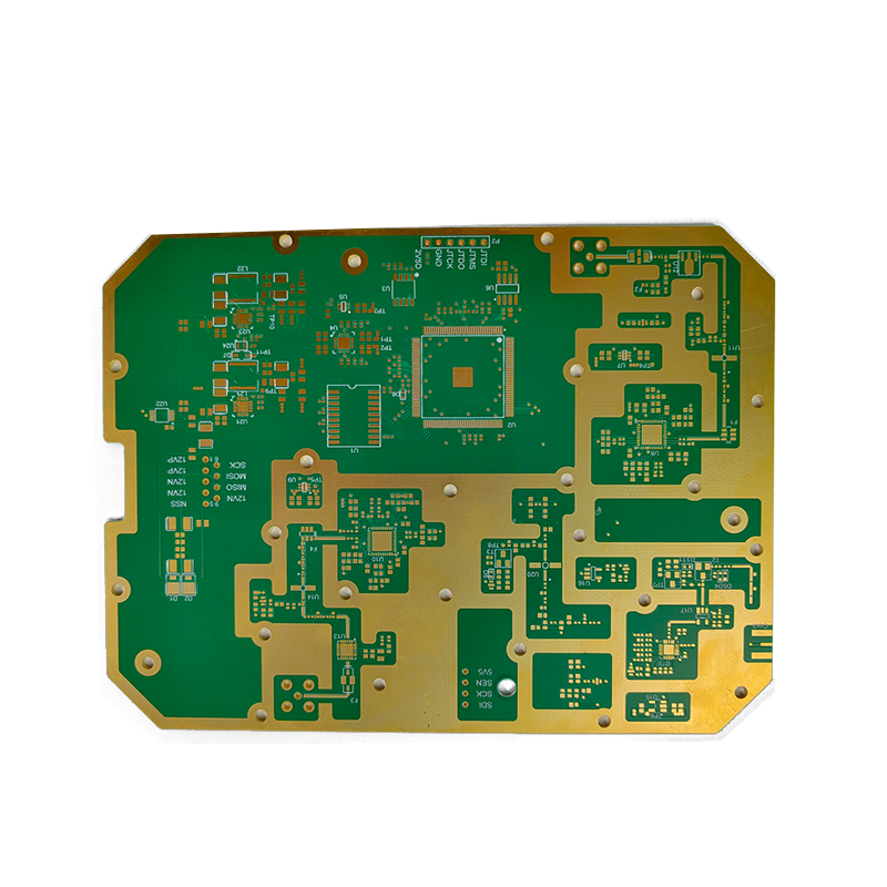
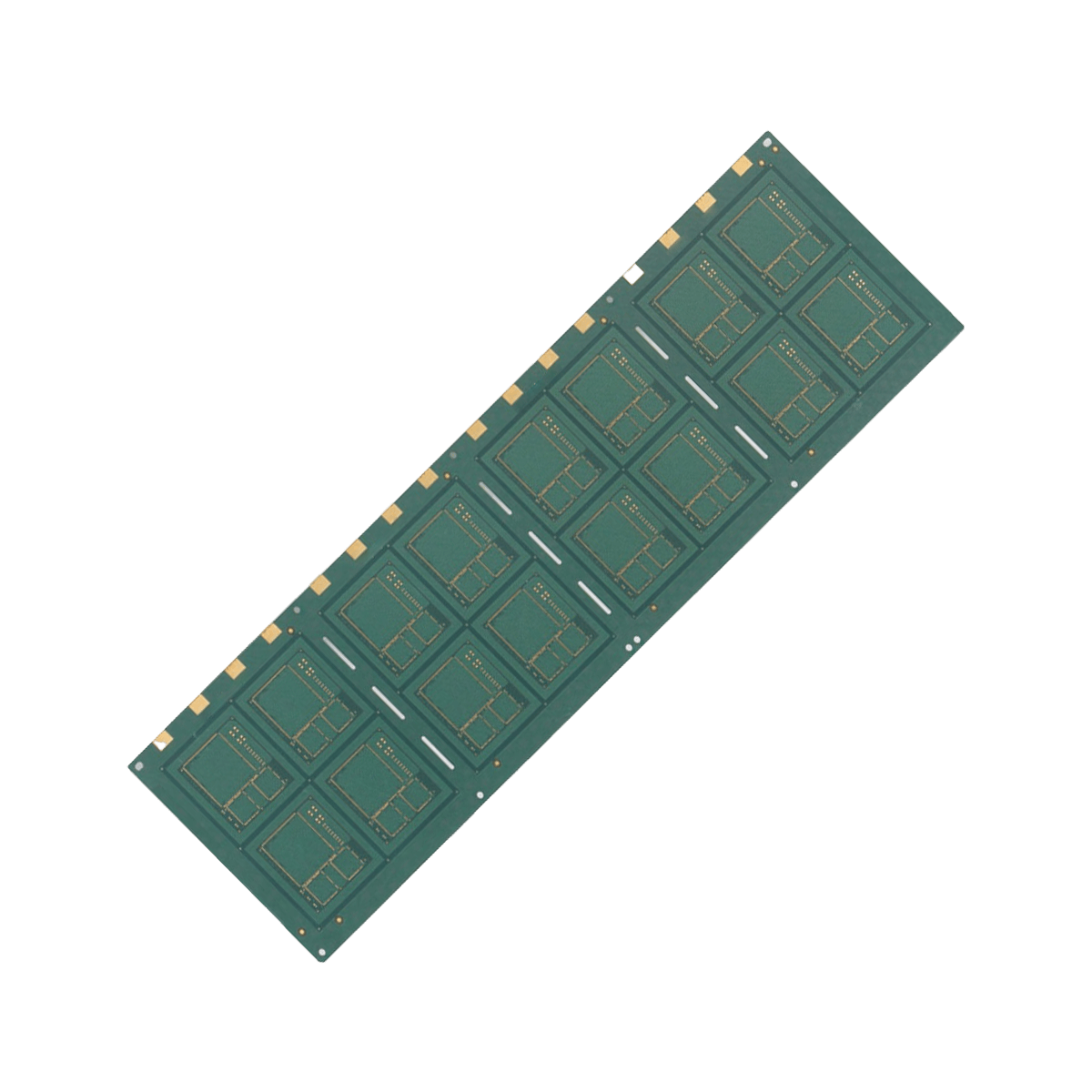
IC Substrate PCB board plays a crucial role in advanced packaging technology and is widely used in mainstream packaging technologies such as BGA, CSP, MCM, and SIP for high-density IC packaging. It provides a connection between the PCB and the IC packages which are built on a Printed Circuit Board.
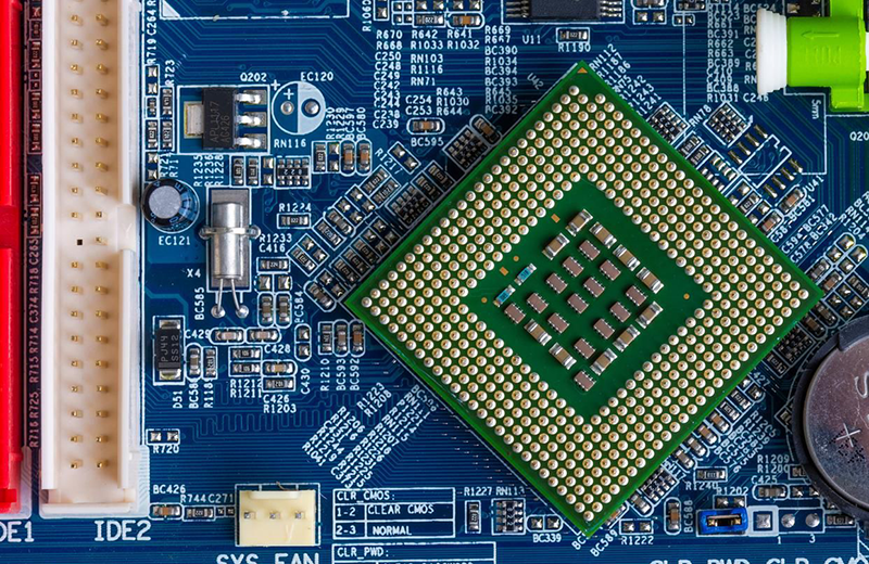
The primary function of the package is to provide shielding for the integrated circuit (IC) from noise reflections, which can significantly affect its performance. The IC core is supported at the center by a multi-layer printed circuitboard (PCB) substrate, which is precision-etched. The manufacturing quality of the IC substrate plays a critical role in determining the overall performance of the IC. IC chip substrates are typically more densely populated than standard high-density PCBs, enabling System on Chips (SoCs) in the IC substrate to offer advantages such as GPIO pins and peripheral connections.
IC substrate PCBs are used in a wide range of applications, including smartphones, tablets, networking devices, compact telecommunication equipment, medical devices, aerospace, aviation, and military technologies. At the system level, they are employed in processors, memory devices, graphics cards, gaming chips, external sockets, and more.

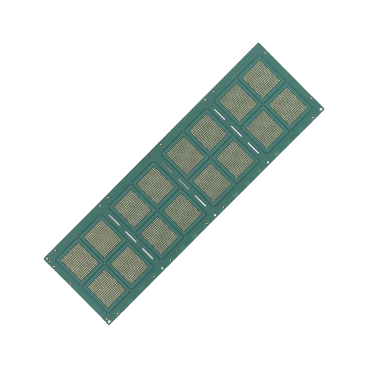
Compared to ordinary PCBs, IC Substrate PCBs have the advantages of thinner board body, finer line width and spacing, smaller aperture, etc., requiring more precise alignment technology, electroplating technology, etc. In addition, it also plays a role in protecting, supporting, dissipating heat, and forming standardized installation dimensions.
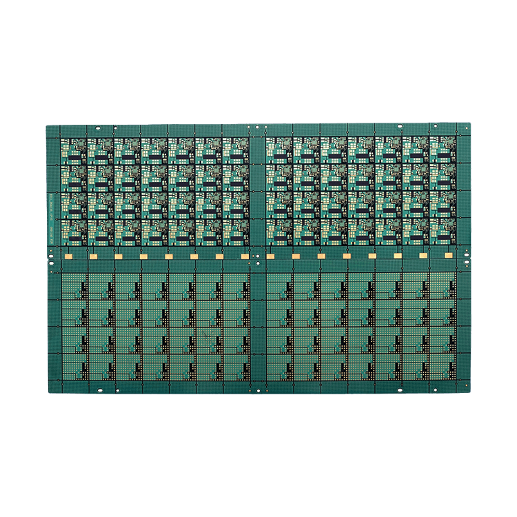
As a high-end PCB board, IC carrier board has the characteristics of high density, high precision, miniaturization, and lightweight, and is widely used in downstream application fields such as mobile terminals, communication devices, services/storage, etc.
The main types of IC substrates:
① Organic IC Substrate
Made from organic materials such as BT resin (Bismaleimide Triazine), FR4, and Polyimide.
Commonly used for System on Chip (SoC) packages, QFN (Quad Flat No-lead), and BGA (Ball Grid Array) packages.
Advantages: Cost-effective, versatile, and compatible with mass production.
Applications: Smartphones, computers, consumer electronics, automotive systems.
② Ceramic IC Substrate
Made from high-performance ceramic materials like Alumina (Al₂O₃), Aluminum Nitride (AlN), and Beryllium Oxide (BeO).
Known for their excellent thermal conductivity and high-temperature resistance.
Advantages: Superior thermal management, better electrical performance, and higher reliability.
Applications: High-power electronic devices, military and aerospace equipment, power modules, and automotive applications.
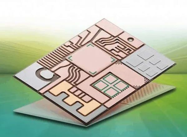
③ Metal-Based IC Substrate
Utilizes metals such as copper, aluminum, or copper-tungsten as the base material, with metal core PCBs (MCPCBs) often used for heat dissipation.
Advantages: Excellent thermal conductivity, enhanced heat dissipation, and robustness.
Applications: Power electronics, LED lighting, and automotive electronics.
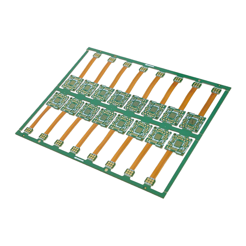
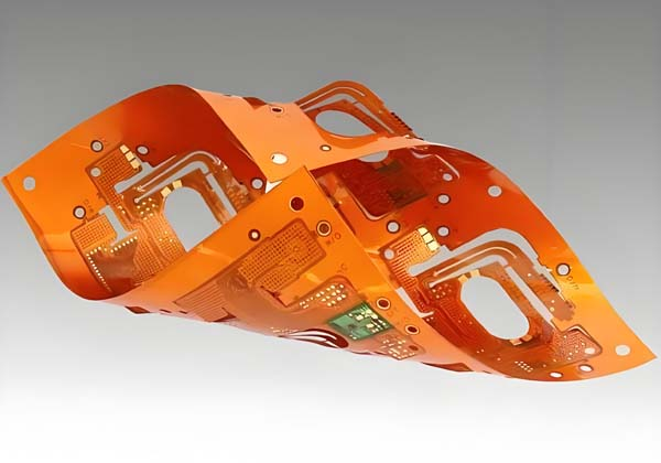
④ Flex and Rigid-Flex IC Substrate
Combines flexible or rigid-flex PCB technology with IC substrates to create more compact and adaptable packaging solutions.
Advantages: Flexibility, space-saving, and reduced weight.
Applications: Wearable electronics, medical devices, aerospace applications, and compact consumer electronics.

⑤ High-Density Interconnect (HDI) IC Substrate
Features fine-pitch technology and micro-via structures for high-density interconnections.
Advantages: Increased circuit density, improved electrical performance, and compactness.
Applications: Mobile devices, high-performance computing, high-frequency communication systems, and other miniaturized electronics.
⑥ Embedded IC Substrate
The IC components are embedded within the PCB itself, creating a more integrated and compact design.
Advantages: Reduced package size, enhanced reliability, and better signal integrity.
Applications: Advanced consumer electronics, automotive applications, and high-performance computing.
⑦ Substrate for Fan-Out Wafer-Level Packaging (FOWLP)
A newer type of packaging where the IC is placed directly onto the substrate, with fan-out redistribution layers created using wafer-level packaging techniques.
Advantages: Low-cost, high-performance, and suitable for small form factors.
Applications: Smartphones, IoT devices, and miniaturized consumer electronics.
It can be classified according to packaging methods, processing materials, and application fields:
(1) According to the packaging method, IC substrates are classified into BGA packaging substrates, CSP packaging substrates, FC packaging substrates, and MCM packaging substrates.
(2) IC carrier boards can be roughly divided into three categories based on their materials:
- Hard substrate: The main materials are BT/ABF/MIS; Its main application areas include: communication and memory chips, LED chips/CPUs, GPUs and chipsets, and a large number of high-end chip/analog, power IC, and digital currency market fields.
- Flexible substrate: The main materials are PI/PE; Its main application areas are automotive electronics, consumer electronics, and can also be applied to military applications such as launch vehicles, cruise missiles, and space satellites.
- Ceramic substrate: The main materials are alumina/aluminum nitride/silicon carbide; And its application fields include semiconductor lighting, laser and optical communication, aerospace, automotive electronics, deep-sea drilling, etc.
(3) According to the classification of application fields, IC carrier boards are divided into storage chip packaging substrates, microelectromechanical system packaging substrates, RF module packaging substrates, processor chip packaging substrates, and high-speed communication packaging substrates.
The IC Substrate Manufacturing Process
1. Material Preparation
- Objective: Prepare base materials like BT resin, polyimide, ceramic, or high-Tg FR4.
- Process:
- Laminates are created by impregnating a dielectric material with resin.
- Copper foil is bonded to form a copper-clad laminate (CCL).
2. Inner Layer Fabrication
- Objective: Create circuit patterns on the inner layers.
- Process:
- Photoresist Application: A photoresist layer is applied to the copper surface.
- Imaging: Circuit patterns are transferred onto the photoresist using photolithography.
- Etching: Exposed copper is etched away to form circuit traces.
- Stripping: The remaining photoresist is removed to reveal the final pattern.
3. Multi-Layer Lamination
- Objective: Stack multiple inner layers to create a multi-layer PCB substrate.
- Process:
- Layers are aligned precisely.
- Heat and pressure are applied to bond layers together using prepreg (resin-coated fiberglass sheets).
4. Drilling
- Objective: Create vias for electrical connections between layers.
- Process:
- Holes are drilled using mechanical drills or laser drilling for microvias.
- Precision is critical to ensure alignment and integrity.
5. Via Formation and Plating
- Objective: Establish electrical connectivity through vias.
- Process:
- Holes are cleaned to remove debris.
- Copper is deposited inside the vias using electroplating or electroless plating methods.
6. Outer Layer Fabrication
- Objective: Form circuit patterns on the outer layers.
- Process:
- Similar to inner layer fabrication, photolithography and etching techniques are used.
7. Surface Finishing
- Objective: Enhance solderability and prevent oxidation.
- Options:
- ENIG (Electroless Nickel Immersion Gold)
- OSP (Organic Solderability Preservative)
- HASL (Hot Air Solder Leveling)
8. Solder Mask Application
- Objective: Protect circuit traces and vias from environmental damage.
- Process:
- Solder mask is applied over the substrate, leaving pads exposed for connections.
9. Surface Marking
- Objective: Add labels, logos, or identifiers.
- Process:
- Silkscreen or laser marking is used for precision.
10. Electrical Testing
- Objective: Verify the functionality and continuity of the circuit.
- Tests:
- Open and short testing.
- Impedance testing for high-frequency applications.
11. Quality Inspection
- Objective: Ensure dimensional accuracy and compliance with specifications.
- Methods:
- Visual inspection.
- Automated Optical Inspection (AOI).
- X-ray inspection for buried or blind vias.
12. Packaging and Shipment
- Objective: Protect the substrate during transport.
- Process:
- Substrates are cleaned, stacked, and vacuum-sealed for shipment.
SysPCB: The best decision for your IC Substrate PCB supplier
SysPCB is one of the IC substrate manufacturers in China.Here’s why choosing us is the best decision for your IC substrate PCB needs:
Fast Turnaround Time
As a leading IC substrate PCB supplier in China, we pride ourselves on delivering high-quality IC substrate PCBs with rapid turnaround times. With our state-of-the-art fabrication and testing equipment, we ensure that your IC substrate are ready quickly, enabling you to bring your products to market sooner and accelerate your return on investment.
Premium Quality PCBs
We are committed to manufacturing only the highest-quality PCBs that meet all industry standards and customer specifications. As trusted PCB prototype manufacturers, we follow established procedures to ensure top-notch performance and reliability. Our continuous improvement approach ensures that we consistently provide better service and quality with every project.
No MOQ
SysPCB does not have a minimum order quantity (MOQ) requirement, so you can confidently partner with us. As an IC substrate PCB manufacturer, we are committed to building long-term relationships based on mutual trust and benefit.
Searching for reliable IC substrate suppliers? Look no further! Contact us today for the perfect quote tailored to your needs!