Table of Contents
What is Teflon PCB?
Teflon PCB board, also known as polytetrafluoroethylene (PTFE) PCB board, is a special type of printed circuit board widely used in the field of high-performance electronics. It is made of polytetrafluoroethylene (PTFE) material, which has excellent electrical and physical properties, making it an ideal choice for high-performance electronic applications.
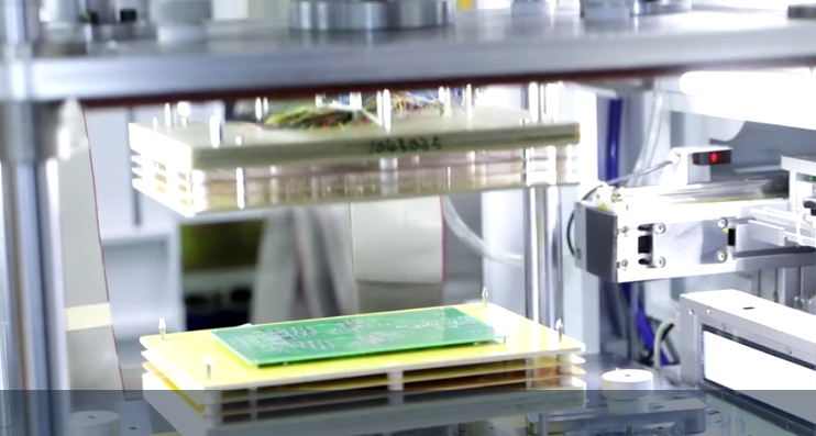
Process flow of PTFE PCB
Material preparation
Firstly, select a suitable substrate and perform pre-treatment. The substrate of PTFE PCB is usually composed of glass fiber cloth and PTFE resin composite. Before processing, it is necessary to clean and pre treat the substrate to ensure its surface flatness and adhesion.
Circuit pattern formation
Transfer the circuit pattern onto the substrate through photolithography technology. The specific steps include coating a photosensitive solder mask material on a PTFE substrate, and then transferring the circuit pattern onto the board through exposure and development processes. This process requires extremely high precision and a clean environment to ensure the accuracy and clarity of the pattern.
Etching process
Etching is a key step in removing excess copper material after forming a circuit pattern. The selection of etching solution and the control of etching time must be precise to avoid damage to the PTFE substrate. Excessive etching may damage the material properties of the circuit board.
Follow up processing
After etching is completed, a series of follow-up processes need to be carried out on the PTFE PCB, including cleaning, drying, and inspection. These steps ensure the cleanliness and absence of defects of the circuit board, preparing it for final electrical testing and assembly.
Surface treatment
Finally, surface treatment is performed to improve the corrosion resistance and conductivity of PTFE PCBs. Common surface treatment methods include tin spraying, gold spraying, and silver spraying.
Preparation process of PTFE coating
(1) Substrate treatment:
Cleaning the surface of the substrate of oil, dust, and other impurities, usually achieved through chemical cleaning or mechanical cleaning. It is also necessary to polish or sandblast the surface of the substrate to increase the contact area between the coating and the substrate and improve adhesion.
(2) Coating preparation:
Select the appropriate PTFE coating and dilute it to the appropriate viscosity, then choose the appropriate coating method (such as spray coating, dip coating, roll coating, etc.) to evenly coat the coating on the surface of the substrate.
(3) Coating curing:
The substrate coated with the coating is cured at a certain temperature, and the curing temperature and time are controlled to ensure that the coating is fully cured. The curing atmosphere (such as oxygen concentration, humidity, etc.) may also affect the performance of the coating.

Application areas of Teflon PCB board
Teflon PCB boards have been widely used in various fields due to their excellent characteristics.
1. Communication equipment
Teflon boards perform well in high-frequency communication devices. Its low dielectric constant and low loss characteristics make it an ideal choice for microwave circuits, radar systems, and satellite communication equipment.
2. RF applications
Teflon PCB boards have excellent performance for RF applications. Its stable dielectric properties and excellent signal transmission capability make it widely used in fields such as wireless communication and radio frequency amplifiers.
3. High temperature environment
Due to the high temperature resistance of Teflon, their application in high-temperature environments is excellent. This includes the aerospace industry, high-temperature industrial equipment, etc.
Advantages of Teflon PCB board
The reason why Teflon PCB boards are highly favored is because of their unique advantages:
1. High temperature stability
Teflon PCB boards can maintain stable performance in high temperature environments and are not easily affected by temperature changes.
2. Low dielectric constant and loss
These characteristics make Teflon boards perform well in high-frequency and RF applications, helping to reduce signal loss and interference.
3. Excellent insulation performance
Teflon PCB board has excellent insulation performance, which can prevent interference and leakage between circuits.
4. Chemical corrosion resistance
Teflon PCB boards have high resistance to many chemicals, making them suitable for various harsh environments.
Disadvantage of Teflon PCB board
1.High cost:
Due to the high material and processing costs, the price of PTFE PCB is relatively high.
2.High processing difficulty:
Due to its special physical and chemical properties, the processing process is relatively complex.

Frequently asked questions
Q1: How high temperature can Teflon PCB board withstand?
Teflon PCB boards can typically withstand temperatures up to 260 ° C and have excellent high-temperature stability.
Q2: What specific fields is this type of PCB suitable for?
Teflon PCB boards perform well in fields such as communication equipment, RF applications, and high-temperature environments.
Q3: Is the manufacturing process of Teflon PCB board complicated?
Yes, the manufacturing process of Teflon PCB boards is relatively complex and requires multiple steps to ensure performance and quality.


Q4: What is the difference between Teflon PCB board and conventional PCB board?
Teflon PCB boards have lower dielectric constant, high temperature stability, and excellent insulation performance, making them more suitable in specific fields.
Q5: How to choose a suitable Teflon PCB board manufacturer?
Choose experienced and reputable manufacturers, understand their product quality and customer feedback to ensure high-quality Teflon PCB boards are obtained.
Why Choose SysPCB to be Your Teflon PCB Board Manufacturer?
SysPCB is a reliable China Teflon PCB manufacturer. We are serving a wide range of clients worldwide on orders ranging from prototypes to mass production. Here are the reasons for choosing SysPCB:
Over a Decade of PCB Fabrication Expertise
With over 10 years of experience in PCB fabrication and assembly, we have earned the trust of many long-term clients who have relied on our services for more than a decade.
Deliver High-quality Teflon PCBs
We ensure top-quality Teflon PCBs by implementing comprehensive processes, including Design for Manufacturability (DFM), electrical testing (E-test), Automated Optical Inspection (AOI), X-ray inspection for BGA, In-Circuit Testing (ICT), and functional testing when required.
No MOQ
Whether you need just a few prototypes or hundreds of fully assembled PCBs, we offer competitive pricing with no minimum order quantity. Contact us today for a free quote!