Table of Contents
What is a Gold Finger PCB?
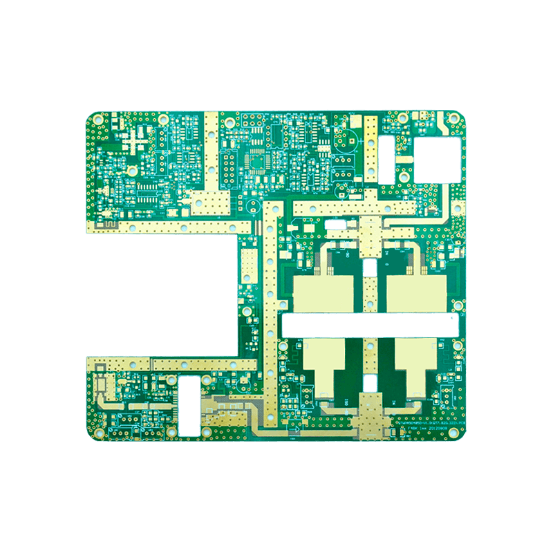
Gold Finger PCB refers to a gold-plated narrow connector that inserts a section of a PCB circuit board into a connector card slot. These connectors use the insertion pins of the connectors as the outbound pins of the circuit board, allowing the solder pads or copper foil to make contact with the corresponding pins at the corresponding positions, thereby achieving electrical connection. Due to the shape of these gold-plated contacts resembling fingers, they are called “golden fingers”.
The influence of rough gold plating:
Decreased electrical performance
Rough surface of gold fingers can increase contact resistance, leading to increased attenuation in signal transmission and potentially causing data transmission error or unstable connection.
Reduced durability
Rough surfaces are prone to accumulate dust and oxides accelerated the wear of the gold layer and reduced the lifespan of the gold fingers.
Mechanical performance damage
Uneven surfaces may scratch the contact points of the other party during insertion and extraction, affecting the tightness of the connection between both parties. In severe cases, it may result in the inability to insert or remove properly.
Decreased aesthetic appeal
Although this is not a direct issue with technical performance, the appearance of the product is also an important reflection of quality, and rough gold plating can affect customers’ overall evaluation of the product.

Acceptance criteria for Gold Finger PCB
In order to ensure the high performance and reliability of the Golden Finger PCB, the industry has established a series of strict acceptance standards, mainly involving the following aspects:
- Gold plating thickness: Generally speaking, the gold plating thickness for gold fingers is required to be between 0.125 μ m and 5.0 μ m, with specific values depending on application requirements and cost considerations. Thin is prone to wear and tear, while thick is too costly.
- Surface roughness: Ra (arithmetic mean roughness) is used as the measurement index, and the common acceptance standard is Ra ≤ 0.10 μ m. This standard ensures good electrical contact and durability.
Coating layer for Gold Finger PCB
- Uniformity: The gold plating layer should be evenly covered without obvious spots, exposed copper, or bubbles to ensure consistent performance at each contact point.
- Solderability and corrosion resistance testing: The corrosion resistance and long-term reliability of gold fingers are tested through methods such as salt spray testing and high temperature and high humidity testing.
The process of Gold Finger PCB mainly includes the following:
1. Chemical nickel immersion gold (ENIG): This process is cost-effective and easy to weld, but it is soft and thin, making it unsuitable for frequent insertion and removal.
2. Electroplating hard gold: This type of gold is solid, with high hardness and thickness (usually 30 microns), suitable for occasions that require frequent insertion and removal.
3. Sinking gold: Suitable for occasions with low wear resistance requirements, with low cost and a conventional thickness of 1-3 microns.

Applications of Golden Finger PCB:
- External Connection: The Golden Finger PCB is used to connect external devices such as speakers, graphics cards, scanners, printers, and monitors.
- Interconnection point: When the auxiliary PCB is connected to the motherboard, the gold fingers play a role in conducting signals, such as PCI, ISA, or AGP slots.
- Special adapters: Special adapters used to enhance computer performance, such as PCBs that enhance graphics and high fidelity sound.
The design features of the Golden Finger PCB include:
(1) Uniform golden fingers: The solder pads have the same length, width, and space, making them suitable for situations that require uniform signal transmission.
(2) Uneven golden fingers: Solder pads with the same width but different lengths, suitable for situations that require different signal transmission strengths.
(3) Segmented gold fingers:With different pad lengths, suitable for electronic products that require waterproofing and durability.
Characteristics difference between immersion gold PCB and gold plating PCB
I: Immersion gold PCB board and electric gold PCB board
1. Immersion gold board and chemical gold board are the same process product, electric gold board and flash gold board are also the same process product. In fact, it is just a different name from different people in the PCB industry. Immersion gold board and electric gold board are more common in the title of the mainland China PCB manufacturers, while the chemical gold board and the flash gold board are more commonly referred to by the Taiwan PCB manufacturers.

2. Immersion gold/chemical gold PCB is generally called chemical nickel gold PCB or chemical nickel immersion gold PCB. The growth of nickel/gold layer is generated by chemical deposition; electro gold PCB /flash gold PCB is generally called electroplated nickel gold PCB or flash gold PCB. The generation of the nickel/gold layer is plated by DC electroplating.
3. Refer to the table below for the difference in mechanism between electroless nickel gold plating (immersion gold) and electroplated nickel gold (gold plating):
| Color Appearance | Solderability | Signal Transmission | Quality | Engineering | |
| Gold plating PCB | Gold with little white | Normal, accidently pseudo solder | conductor skin effect, not good for high frequency signal | 1. Gold surface is easy oxidize 2. Gold wire may cause short3. Bonding stress with soldermask is not good | No need Line Compensation, suit for small space |
| Gold immersion PCB | Gold | good | conductor skin effect is small | 1. Gold surface is not easy oxidize 2. No gold wire 3. Bonding stress with soldermask is good | Need Line compensation |
II: Why do not use “HASL” for high end PCB?
1. As the integration level of IC becomes higher and higher, IC pins become denser. The vertical spray tin process is difficult to flatten the thin pads, which brings difficulty to the SMT process; in addition, the shelf life of the HASL PCB is very short. The immersion gold board just solves these problems
2. For the surface mount process, especially for 0603/0402 or ultra-small surface mount chips, because the flatness of the pad is directly related to the quality of the solder paste printing process, it has a decisive influence on the quality of the subsequent reflow soldering, so the gold immersion is common in high-density and ultra-small surface mount processes.

3. In the PCB prototype production stage, due to factors such as component procurement, it is often that the board is not soldered immediately, but it is often used for several weeks or even months. The shelf life of the gold-plated board is longer than that of lead-tin board, so everyone is willing to use it. Besides, the cost of the gold-plated PCB in the sample stage is almost the same as that of the HASL PCB board. But as the wiring becomes denser, the line width and spacing have reached 3-4mil, gold plating process also brings about the problem of short circuit of gold wire.
As the frequency of the signal gets higher and higher, the skin effect of signal transmission in the multi-plated layer has more obvious influence on the signal quality:
The skin effect refers to: high frequency alternating current, the current will tend to concentrate on the surface of the wire to flow. According to calculations, skin effect depth is related to frequency.
SysPCB: A Reliable Gold Finger PCB Supplier
We prioritize our customers, offering exceptional support and prompt responses to inquiries at any time. Here’s why SysPCB is the ideal choice for your gold finger PCB needs:
No MOQ
SysPCB does not have a minimum order quantity (MOQ) requirement, so you can confidently partner with us. As an gold finger PCB manufacturer, we are committed to building long-term relationships based on mutual trust and benefit.
One-Stop Service
If you’d like to avoid the hassle and skip some steps, you can opt for our one-stop turnkey service. SysPCB can manage the entire process for you, with clear and transparent workflows that help save you time and effort. Once the order is placed, all you need to do is wait for the delivery of your goods.
Comprehensive Pre-Sales and After-Sales Support
SysPCB offers dedicated pre-sales support with a professional customer service and technical team available to assist with any inquiries or consultations at your convenience. Post-sales, we are committed to addressing any quality issues by offering rework services or appropriate compensation. Ensuring a positive customer experience is a core value of our company, and we strive to provide exceptional service at every stage of your engagement with us.