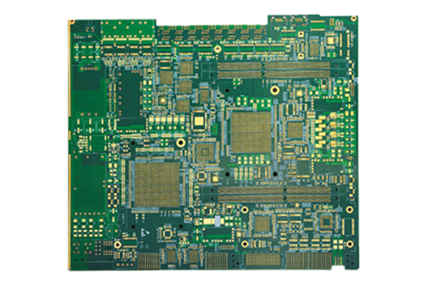
Printed Circuit Boards (PCBs) rely on different types of vias to establish electrical connections between layers. Among them, blind holes and buried holes are critical in high-density and multilayer PCB designs. These specialized vias enable compact layouts, improve signal integrity, and enhance overall PCB performance. This article explores the characteristics, manufacturing process, and applications of blind and buried holes in PCB fabrication.
Table of Contents
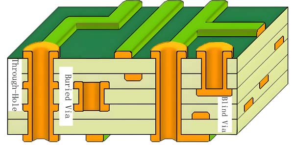
1. What Are Blind and Buried Holes?
Blind Holes: These are vias that connect an outer layer of the PCB to one or more inner layers but do not pass through the entire board. They help optimize space and enhance signal integrity.
Buried Holes: These are vias completely enclosed within the internal layers of a PCB, without extending to the outer layers. They enable higher routing density without affecting surface components.
2. What are the manufacturing processes for blind holes and buried holes?
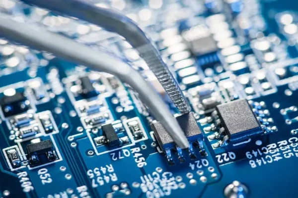
– Blind Hole Manufacturing
Drilling: Laser drilling or mechanical drilling creates precise hole structures between the required layers.
Plating: Copper is electroplated onto the via walls to establish conductivity.
Lamination: The PCB stack-up is assembled, ensuring the blind via is positioned correctly between layers.
Etching & Surface Treatment: The board undergoes chemical processing to define conductive paths and improve solderability.
– Buried Hole Manufacturing
Inner Layer Fabrication: The inner layers are processed first, including etching and drilling.
Lamination: After the buried vias are drilled and plated, the layers are pressed together to form the complete PCB stack-up.
Plating & Conductivity Testing: Additional plating ensures a reliable electrical connection between the internal layers.
3. What are the advantages of blind holes and buried holes?
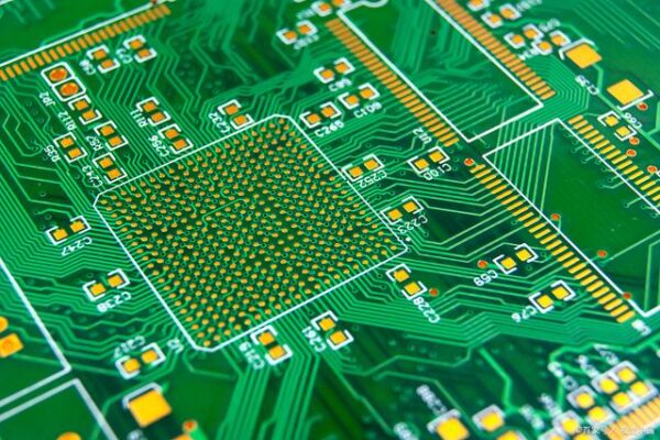
High-Density Interconnect (HDI) Support: Enables more compact and complex designs, particularly for HDI PCBs.
Enhanced Signal Integrity: Reduces signal distortion by minimizing unnecessary via stubs and optimizing routing.
Space-Saving Design: Frees up surface area for component placement, allowing for miniaturization of electronic devices.
4. What are the common applications for blind holes and buried holes?
Smartphones and Tablets: High-density PCB designs in mobile devices benefit from blind and buried vias for compactness and performance.
Automotive Electronics: Advanced driver assistance systems (ADAS) and infotainment units require multilayer PCBs with efficient routing.
Medical Devices: Miniaturized medical electronics, such as imaging and monitoring systems, utilize blind and buried vias for space efficiency.
Aerospace and Defense: High-reliability PCBs in military and aerospace applications depend on precise via structures for optimal performance.
Conclusion
Blind and buried holes are essential for modern PCB designs, particularly in multilayer and HDI applications. Their implementation enhances space utilization, signal integrity, and overall PCB efficiency. However, the complexity of manufacturing these vias adds to production costs and requires advanced fabrication techniques. Understanding their role and benefits allows PCB designers to make informed choices for high-performance electronic applications.
Get your exclusive quote immediately: fill out the form or send an email directly.As a professional PCB manufacturer for hobbyist , we will provide you with a quote service within 24 hours. Enjoy free DFM optimization and a 10% discount on SMT patches for your first order!