When designing PCB, please pay special attention to these 5 points to ensure circuit performance, reliability, and manufacturability:
Table of Contents
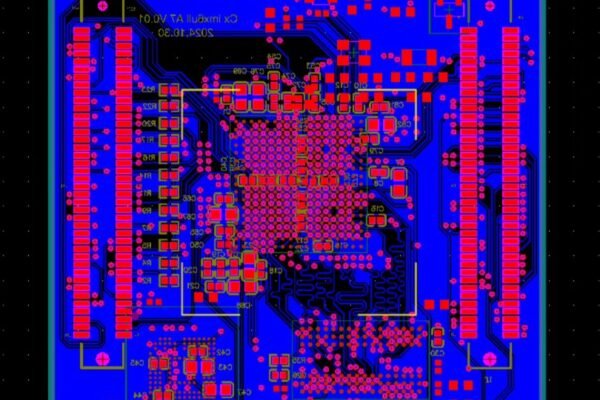
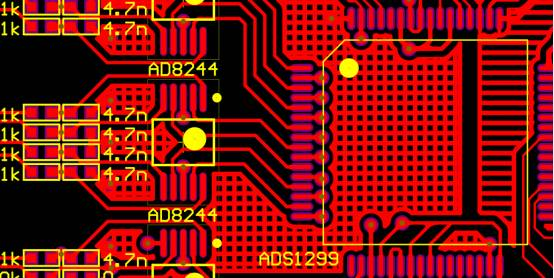
1. Component layout and partitioning
-Functional zoning
Separate the layout of analog circuits, digital circuits, and high-frequency/low-frequency modules to avoid signal interference (such as digital noise affecting analog signals).
-Key component locations
Sensitive components such as crystal oscillators, inductors, antennas, etc. should be kept away from noise sources (such as power modules) and the high-frequency signal path should be minimized as much as possible.
-Heat dissipation considerations
High power components such as MOS transistors and power chips need to reserve heat dissipation space to avoid temperature rise caused by concentrated heating.
2. Power and ground wire design
-Power integrity
When using multi-layer boards, design independent power layers and ground planes to reduce power impedance and loop interference.
-Decoupling capacitor
Place high-frequency/low-frequency decoupling capacitors (such as 0.1 μ F and 10 μ F combinations) near the power pins to filter out high-frequency noise.
-Ground segmentation and connection
To avoid ground plane breakage, the ground of different functional modules can be connected through a single point (such as magnetic beads or 0 Ω resistors) to reduce common ground interference.
3. Signal integrity and high-speed signal processing
–Impedance matching
High speed signal lines (such as USB, HDMI, DDR) need to be designed according to their characteristic impedance (such as 50 Ω or differential 100 Ω) to avoid signal reflection.
-Wiring rules
When designing PCB, it is necessary to shorten the high-speed signal path, avoid right angle wiring (use 45 ° or circular arc instead), and reduce crosstalk and electromagnetic radiation.
-Differential pair and equal length wiring
Maintain symmetrical routing for differential signals (such as LVDS, PCIe), and perform equal length processing on critical timing signals.
4. Thermal management design of PCB
-Heat dissipation channel
Add heat dissipation holes (Via), heat sinks, or reserved heat dissipation pads for high-power components.
-Copper foil area
By laying copper or increasing copper thickness, the heat dissipation ability can be improved to avoid local overheating.
-Air circulation
In a closed environment, the layout of components should consider the direction of air flow to avoid the heat island effect.

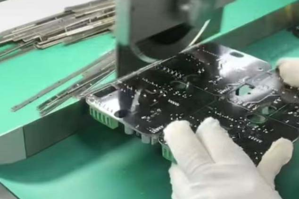
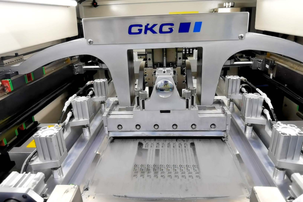
5. Requirements for PCB manufacturing and assembly process
-Line width/spacing
meets the minimum process capability of PCB manufacturers (such as conventional 6/6mil, high-precision 4/4mil).
-Aperture and solder pad
The size of the through-hole and solder pad should be adapted to the component pins to avoid virtual soldering or assembly conflicts.
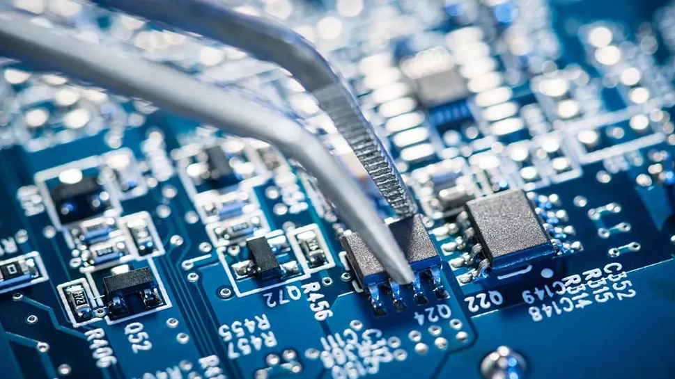
-Screen printing and labeling
Clearly label component polarity, test points, and key signals for easy debugging and maintenance.
Summarize
When designing PCB, please pay special attention to these 5 points mentioned in the blog, as they will directly affect the performance, EMC (electromagnetic compatibility), and feasibility of mass production of the circuit board. When designing PCB, it is necessary to combine simulation tools (such as SI/PI analysis) and design specifications (such as IPC standards), and communicate process details with manufacturers before board placement to reduce rework risks.