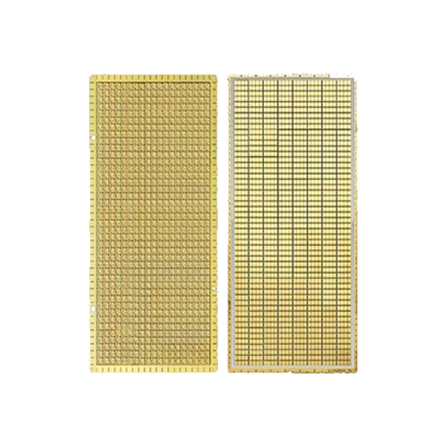
The manufacturing process of ceramic PCB varies depending on its materials and process technology, mainly divided into thin film process, thick film process, direct bonding copper (DBC) process, laser assisted metallization (LAM) process, and arc spraying process. Let’s start introducing the manufacturing process of ceramic PCB:
Table of Contents
Applicable scenarios of different processes
| workmanship | characteristic | application area |
| Thin Film Process (DPC) | High precision, high frequency, high density, but high cost | RF devices, optical communication modules |
| Thick film process (HTCC) | High temperature resistance, multi-layer integration, but high energy consumption | Aerospace electronics, high-temperature sensors |
| DBC process | High current carrying capacity, high reliability, limited materials | High power IGBT modules, electric vehicles |
| LAM process | Ultra high thermal conductivity, 3D wiring, high cost | High power LED, 5G base station |
| Arc spraying process | Low cost, strong material compatibility, simplified process | Low to medium power supply module, industrial control |
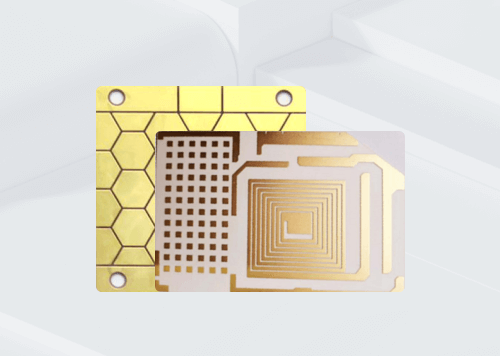
1、 Thin film process (such as DPC process)
The thin film process is suitable for ceramic PCBs with high-precision and ultra-fine circuits, and the core steps include:
1. Substrate cleaning
Remove oil stains and impurities on the surface of ceramic substrates through ultrasonic cleaning.
2. Magnetron sputtering metallization
Sputtering metal (such as titanium, nickel, copper) on the surface of ceramics to form a conductive layer, with a thickness usually less than 1 μ m.
3. Lithography and patterning
Coating photoresist and transferring circuit patterns onto a substrate through exposure and development.
4. Electroplating thickening
The copper layer is thickened to over 10 μ m through electroplating technology to meet the current carrying requirements.
5. Etching and debonding
Remove excess metal and preserve the designed circuit pattern.
6. Drilling and Plating Through Holes (PTH)
After mechanical drilling, interlayer conductivity is achieved through chemical copper plating.
7. Coating of solder mask
Use photosensitive solder mask ink to protect non welding areas and ensure welding reliability.
Features
High resolution (line width/spacing up to 10 μ m), suitable for high-frequency, high-density circuits, but with complex processes and high costs.
2、 Thick film process (HTCC/LTCC/DBC)
Thick film technology achieves the bonding of metal and ceramic through high-temperature or low-temperature sintering:
1. HTCC (High Temperature Co fired Ceramics):
-Mix ceramic powder with adhesive to form a circuit by screen printing metal paste (such as tungsten, molybdenum).
-Sintering at high temperatures above 1600 ° C, co firing metal and ceramic to form a multi-layer structure.
-Application: High temperature and high-frequency scenarios (such as aerospace electronics).
2. LTCC (Low Temperature Co fired Ceramics):
-Use low-temperature sintered ceramic materials (such as glass ceramics) with metal paste of silver or copper.
-The sintering temperature is about 850 ° C, suitable for integrating passive components such as resistors and capacitors.
-Applications: RF modules, sensors.
3. DBC (Direct Copper Bond):
-Copper foil is bonded to ceramics (Al ₂ O ∝ or AlN) through eutectic reaction at high temperature (1065 ° C).
-Etch copper foil to form circuit patterns.
-Characteristics: Combined with high strength and high current carrying capacity, but limited to specific ceramic materials.
3、 LAM process (laser assisted metallization)
LAM technology combines laser processing and metallization processes, suitable for high thermal conductivity requirements:
1. Laser activation: By using laser to generate microstructures on ceramic surfaces, metal adhesion is enhanced.
2. Metal layer deposition: Magnetron sputtering or electroplating to form a copper layer with adjustable thickness (1 μ m-1mm).

3. Laser etching: Use ultraviolet laser to directly etch circuit patterns with an accuracy of up to 20 μ m.
4. 3D wiring: supports complex 3D substrate design.
Advantages:
-Thermal conductivity up to 230 W/m · K (aluminum nitride substrate);
-Combined with high strength (45 MPa), it can be welded multiple times;
-Suitable for high-power LED and power electronic modules.
4、 Arc spraying process (New low-cost ceramic PCB manufacturing process)
In response to the limitations of traditional processes, the arc spraying method proposes an innovative process:
1. Substrate pretreatment: Heat the ceramic in a reducing atmosphere to 350-400 ° C to enhance surface activity.
2. Spray metal layer: Arc spray the bottom layer (aluminum/zinc) and copper layer in sequence, with thicknesses of 10-20 μ m and 15-30 μ m, respectively.
3. Grinding and etching: After grinding the copper layer flat, use ultraviolet laser to etch the circuit pattern.
4. Cutting and testing: Laser cutting is used to produce finished products, and electrical testing is conducted.
Advantages:
-Low processing temperature (<400 ° C), suitable for various ceramic materials;
-Combined with high strength, the cost is reduced by more than 30% compared to DBC.
5、 Supplementary Manufacturing Process for General Ceramic PCB
Regardless of the process used, the following steps typically run through the manufacturing process:
1. Design verification
Use EDA software to complete circuit layout and thermal simulation.
2. Layering and Drilling
Multi layer ceramic substrates need to be laminated and drilled to ensure interlayer conductivity.
3. Surface treatment
Chemical gold or silver plating to improve solderability and oxidation resistance.
4. Electrical testing
Ensure circuit connectivity through flying pin testing or AOI inspection.