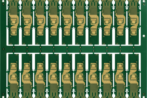
In the fields of high-speed communication, intelligent terminals, and industrial control, 6 layer PCBs have become the preferred solution for complex electronic devices due to their excellent signal integrity, anti-interference ability, and cost-effectiveness. This article provides an in-depth analysis of the core technologies and practical strategies of 6 layered boards, from stacked design and high-frequency optimization to typical industry applications.
Table of Contents
1、 The core advantages and applicable scenarios of 6 layer PCB
1. Signal integrity assurance
The stacked structure of 6 layer PCBs (such as TOP-GND Signal PWR-GND-BOTTOM) forms an electromagnetic shielding “sandwich” through dual ground planes, which can reduce power impedance by 40% and effectively reduce reflection and crosstalk of high-speed signals (such as DDR4, PCIe).
2. High density wiring capability
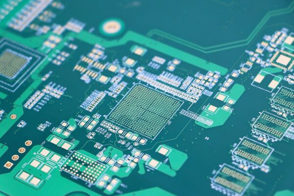
Compared to the four layer board, the 6 layer PCB adds two signal layers, supports BGA packaging and HDI micro hole technology, increases wiring density by 30%, and meets high integration requirements such as 5G modules and AI chips.

3. Widely used in the industry
-Communication equipment: Supports high-speed signal transmission of 10Gbps or more, suitable for base station RF modules;
-Automotive electronics: meet the stringent requirements of ADAS systems for high temperature resistance and vibration resistance;
-Medical equipment: Ensure signal stability of precision instruments through EMC optimization.
2、 The Golden Rule of Stacking Design and Power Optimization
Recommended stacked architecture:
-Plan A (Dual Ground Plane): TOP (Signal) → GND → Signal → PWR → GND → BOTTOM (Signal)
Advantages: Strong electromagnetic shielding, impedance fluctuation<0.1 Ω, suitable for high-speed buses such as DDR.
-Option B (Cost Optimization): TOP (High Speed Signal) → GND → Split Power Layer → Signal → Signal → BOTTOM (High Current)
By using cellular power segmentation and virtual ground plane, power noise can be reduced by 30%.
Key points of power processing:
-Copper foil thickness: High current modules (such as motor drives) need to be upgraded to 2oz to reduce the 10A path temperature rise by 8 ℃;
-Decoupling capacitor layout: 0.1 μ F ceramic capacitors (spacing ≤ 5mm) and 10 μ F tantalum capacitors are arranged in a “honeycomb” pattern around the BGA.
3、 Key Technologies for High Frequency Signal Optimization
1. Impedance matching and wiring rules
-Control the impedance of microstrip/strip lines (50 Ω single ended/100 Ω differential), avoid sharp angle routing, and use 45 ° or circular arc angles;
-Key signals (such as clock lines) should be prioritized in the GND reference layer, maintaining a 3-fold line distance from the power layer to reduce jitter by 15ps.
2. EMC protection design
-Sensitive signals are processed using a “ground wrapping” approach, with ground wires arranged on both sides;
-Avoid signal lines crossing the power/ground plane dividing groove to prevent the backflow path from breaking.
3. Heat dissipation and reliability enhancement
-Arrange through holes under the heating element and use copper foil for heat conduction;
-The via matrix design (4 vias per square centimeter, diameter ≥ 0.3mm) reduces path impedance by 50%.
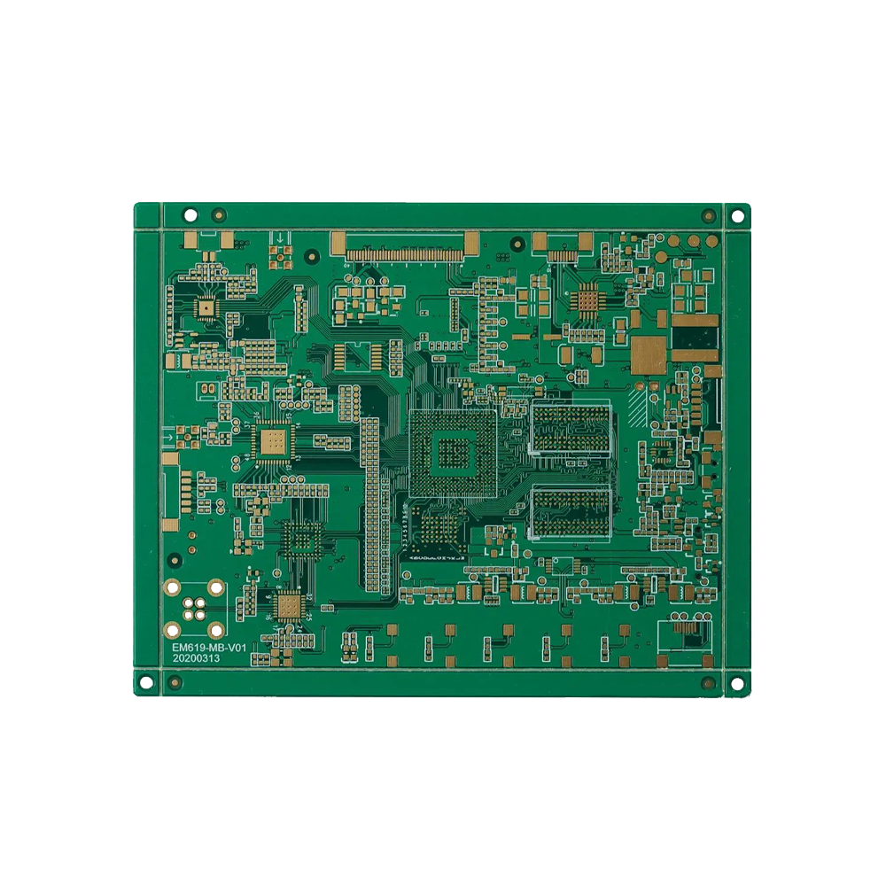
4、 Industry practical cases and DFM suggestions
1. 5G communication module
Using blind buried hole technology to shorten the signal path, combined with HyperLynx simulation tool to optimize the eye diagram quality, the insertion loss is less than 3dB.
2. Automotive ECU control board
Reserve 50mil isolation tape at the edge of the board, form an “electromagnetic moat” through grounding holes, and use high-temperature resistant materials (Tg ≥ 170 ℃) certified by TS16949.
DFM specification:
-Line width/spacing ≥ 5mil, through-hole inner diameter ≥ 8mil;
-Avoiding the false eight layered structure (adding light plates to the middle layer) and reducing manufacturing costs by 20%.