In today’s rapidly developing high-speed electronic devices and communication technology, 4 layer PCBs have become the preferred solution in fields such as industrial control, consumer electronics, and medical equipment due to their excellent performance and cost balance. This article will reveal the core technical points of 4 layer PCBs from the perspectives of design advantages, stacked structures, and high-frequency applications.
Table of Contents
1、 The core advantages of a 4 layer PCB
1. EMC performance improvement
Compared to double-sided panels, 4 layer panels can reduce electromagnetic interference (EMI) by more than 20dB through a complete power layer and ground plane design. The large-area copper foil in the middle layer not only provides stable power supply, but also shields crosstalk between signal layers.
2. More precise impedance control
The outer signal line of the 4 layer PCB forms a “microstrip line” structure with the adjacent ground plane, and its impedance can be accurately calculated through parameters such as line width and dielectric thickness, making it suitable for high-speed signal transmission.
3. Wiring flexibility and density optimization
After adopting a layered design, the power and ground lines are independently layered, freeing up more wiring space, especially suitable for high-density IC (such as BGA packaging) layouts.
2、 Key strategies for designing stacked structures
The typical stacked architecture of a 4 layer PCB can be divided into two types:
-Signal ground power signal: The advantage lies in the close coupling between the signal layer and the ground plane, reducing signal delay and making it suitable for high-frequency scenarios.
-Ground signal power: The ground plane is located on the top layer to enhance electromagnetic shielding, but attention should be paid to crosstalk control between the middle signal layers.
Design points:
-Using a negative plane layer to process power and ground planes reduces data volume and improves processing efficiency.
-Optimize the heat dissipation path through thermal fluid simulation to avoid heat accumulation in the intermediate layer.
3、 Key Technologies in High Frequency Applications
1. Impedance consistency optimization
-Avoid sharp angle wiring and adopt circular arc or 45 ° angle design to reduce local impedance transients (insertion loss can be reduced by 3-5dB).
-Key signal lines (such as clock lines) should be kept away from the ground plane segmentation area to prevent radiation interference.
2. Signal integrity assurance
-The routing directions of adjacent signal layers are orthogonal to reduce interlayer crosstalk.
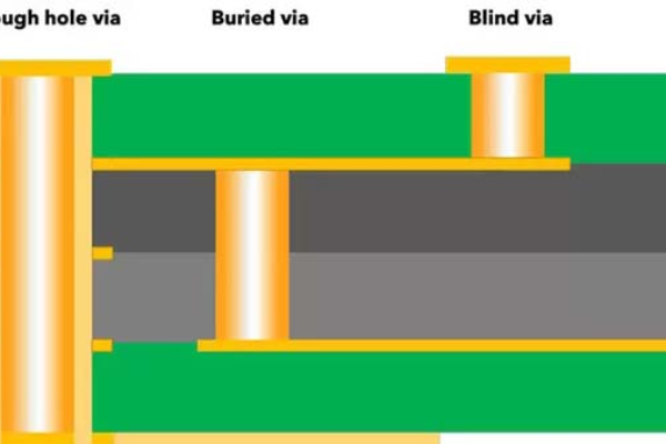
-Using blind buried hole technology to shorten the critical signal path and reduce the impact of parasitic inductance.
3. Mixed grounding design
Combining single point grounding (analog circuit) with multi-point grounding (high-frequency module), different ground planes are connected through magnetic beads or capacitors to balance noise and impedance.

4、 Practical points of 4 layer PCB design
1. Through hole treatment: Avoid drilling holes directly on the solder pad to prevent solder leakage in the chip; Priority should be given to using large-sized power/ground vias (such as 20Mil pads) to reduce impedance.
2. Heat dissipation design: A through hole is arranged below the heating element, using copper foil to conduct heat and enhance structural stability.
3. DFM compatibility: The recommended line width/spacing is ≥ 6mil, and the through-hole inner diameter is ≥ 8Mil, suitable for most board factory processes.
If you need further information on 4 layer PCB design services, please feel free to contact our engineering team!