In the precise “body” of a computer, printed circuit boards (PCBs) are like invisible veins, supporting the efficient operation of various core components. The requirements for PCB vary greatly among different components. Below, we will analyze in depth the characteristics of PCB types, processes, and other features from the motherboard PCB of a computer, the PCB in a graphics card, the PCB in a memory module, and the PCB in a power supply.
Table of Contents
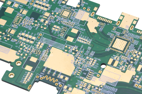
1、 Computer motherboard PCB
(1) Types of motherboard PCBs
1. Multi layer board is mainstream: As the core hub of the entire computer, the computer motherboard integrates numerous key electronic components, so multi-layer board is the main type of motherboard PCB. Usually, motherboards adopt multi-layer board designs of 6, 8, or even 12 layers. Taking the 6-layer board as an example, in addition to the top and bottom layers used for installing electronic components, the middle layer also includes a power layer, a ground layer, and a signal layer. This structure not only meets complex wiring requirements, but also effectively isolates power and data signals, reducing interference.

2. Application of high-density interconnect (HDI) boards: With the continuous integration of motherboard functions and the gradual reduction of size, HDI boards are becoming increasingly widely used on high-end motherboards. HDI boards achieve smaller through holes, finer lines, and higher wiring density through technologies such as laser drilling and electroplating filling. For example, some ultra-thin laptop motherboards that use HDI technology can integrate a large number of components such as CPUs, memory controllers, high-speed interfaces, etc. in limited space, while ensuring the stability of signal transmission.
(2) Process characteristics of Computer PCB
1. Fine line processing technology: To meet the requirements of high-speed signal transmission, the motherboard PCB adopts fine line processing technology. By optimizing the etching process parameters, the line width and spacing can reach tens of micrometers or even smaller. At the same time, processes such as chemical copper plating and electroplating thickening are used to ensure good conductivity and reliability of the circuit, guaranteeing the accuracy of data transmission between high-speed components such as CPU and memory.
2. Surface treatment process: Common surface treatment processes for motherboard PCBs include immersion gold, OSP (Organic Solderable Protective Agent), etc. The gold deposition process deposits a layer of gold on the surface of the PCB, which has good oxidation resistance and solderability, and can improve the reliability of component soldering. It is commonly used in interface areas with high reliability requirements; The OSP process forms an extremely thin organic protective film on the copper surface, which is cost-effective and does not affect the insulation performance of the PCB, making it suitable for large-scale production.
2、 PCB in graphics card
(1) Types of graphics card PCBs
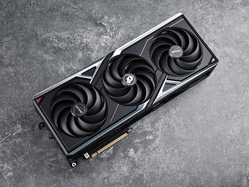
1. Multi layer high-performance board: Graphics cards need to process a large amount of graphics data, and have extremely high performance requirements for PCBs, so multi-layer high-performance PCBs are usually used. The common number of layers in graphics card PCBs ranges from 4 to 8. Increasing the number of layers provides more ample wiring space for core components such as GPUs and graphics memory, while also helping with heat dissipation and signal integrity. For example, the PCB of a high-end gaming graphics card may adopt an 8-layer design, with a dedicated independent power layer to provide stable power supply for the GPU and graphics memory.
2. Auxiliary application of flexible circuit board (FPC): In some specially designed graphics cards, it is used in conjunction with FPC. For example, in order to achieve the three-dimensional stacking design or reduce the volume of graphics cards, FPC can be used to connect different modules of graphics cards, such as transmitting signals from PCB to vertically installed video memory modules, which increases the flexibility of graphics card design and can also reduce electromagnetic interference to a certain extent.
(2) Key process points for graphics card PCB
1. High current carrying capacity process: The GPU and graphics memory components of the graphics card require a large amount of power consumption during operation, so the graphics card PCB needs to have high current carrying capacity. By increasing the thickness of copper foil and optimizing the design of power supply circuits, the PCB can ensure stable power supply to components. In addition, a multi-phase power supply design will be adopted to decompose large currents into multiple small currents, improving the stability and efficiency of power supply.
2. Heat dissipation optimization process: Graphics cards generate a large amount of heat during operation, and the heat dissipation performance of PCBs is crucial. In addition to designing heat dissipation holes on the PCB and increasing the area of heat dissipation copper foil, special heat dissipation materials and processes will also be used. For example, coating a heat dissipation coating on the surface of the PCB or closely adhering it to a metal heat sink can help dissipate heat quickly and ensure the stability of the graphics card during high load operation.
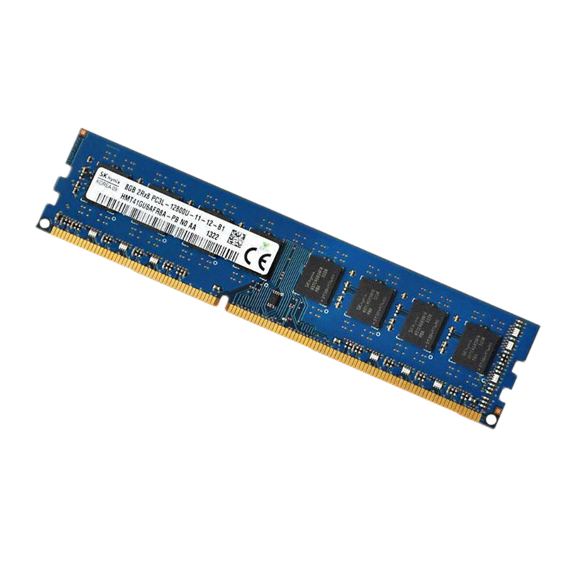
3、 PCB of memory module
(1) Common types of memory module PCBs
1. Multi layer board with double-sided layout: Memory module PCBs usually use 4-8 layer multi-layer boards, and are mostly double-sided layouts, to install memory chips and other electronic components. This design can fully utilize the space of PCB, improve the integration and performance of memory. For example, common 8GB or 16GB memory modules achieve high-capacity storage by installing memory chips on both sides of the PCB.
2. Impedance matching optimization board: Due to the extremely fast data transmission speed of memory and high requirements for signal integrity, the memory module PCB will undergo strict impedance matching optimization. By precisely controlling parameters such as line length, width, and interlayer distance, it ensures that memory signals do not experience reflection, attenuation, or other issues during transmission, thereby ensuring the accuracy and stability of memory data reading and writing.
(2) Process characteristics of memory module PCB
1. High precision soldering process: The memory chips and other components on the memory module are small in size and have dense pins, requiring high-precision soldering process. At present, mainstream memory module production adopts reflow soldering technology, which controls the heating curve to melt the solder paste at a precise temperature, achieving reliable connection between the chip and PCB. Meanwhile, utilizing automated welding equipment can improve the consistency and yield of welding.
2. Gold finger technology: The gold finger part of the memory module is the key part connected to the motherboard memory slot, and its process quality directly affects the stability of the memory. Gold fingers usually use electroplating technology to deposit a uniformly thick layer of gold on the copper surface. The metal has good conductivity, oxidation resistance, and wear resistance, which can ensure good contact between the memory module and the motherboard and reduce faults caused by poor contact.
4、 PCB in power supply
(1) Types of power PCB
1. Single or double-sided board basic type: For some power supplies with relatively low power and simple functions, such as ordinary adapter power supplies, single-sided or double-sided boards are usually used. These PCB structures are relatively simple, cost-effective, and can meet basic power conversion and circuit control requirements. Single or double-sided panels can achieve power input, output, and simple overvoltage and overcurrent protection functions through reasonable layout.
2. Multi layer power dedicated board: In the computer’s main power supply, due to the need for complex power conversion and stable power supply, multi-layer power dedicated PCB is generally used. Multilayer boards can better isolate circuits with different voltages and currents, avoiding mutual interference. For example, arranging the AC input circuit, DC output circuit, and control circuit on different layers can improve the safety and reliability of the power supply.
(2) Key process points of power PCB
1. High voltage insulation process: The power PCB needs to handle high voltage inputs, so insulation process is crucial. By using substrate materials with good insulation properties, increasing the insulation spacing between circuits, and applying insulation paint to key areas, safety hazards such as leakage and short circuits are prevented, ensuring user safety during use.
2. High current processing technology: The power supply generates a large current when outputting power. To ensure that the PCB can withstand the high current, processes such as thickening copper foil, increasing the number and size of vias, etc. are used to reduce circuit resistance and minimize heat generation. At the same time, reasonable layout of power lines, optimization of current paths, and improvement of power conversion efficiency and stability.
The above analyzes the PCB of key computer components from multiple perspectives. If you wish to include our company’s product advantages, technological strength, and other content in the article, please feel free to let me know at any time.