Due to their complex structure and numerous production stages, the performance and reliability of multilayer printed circuit boards (PCBs) are highly dependent on process control throughout the entire manufacturing workflow. Below, we outline critical considerations across key dimensions—from design collaboration and material selection to core processes and quality validation:
Table of Contents
I. Design Collaboration: Mitigating Production Risks at Source
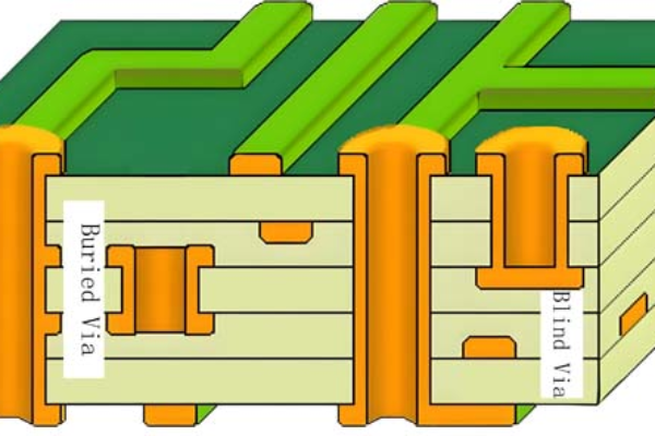
1. Verification of Stack-up Structure Rationality
Multilayer stack-up design must allocate layers based on signal types (high-speed signals, power/ground planes, low-frequency signals): Power and ground planes should be tightly coupled (minimized spacing) to reduce impedance, while high-speed signal layers must be adjacent to reference planes (minimizing signal reflection). Simultaneously, the total thickness and layer thickness ratios (e.g., substrate-to-copper foil matching) must be calculated to prevent delamination caused by uneven stress during lamination.
Additionally, confirm production capabilities (e.g., maximum layers, minimum line width/spacing, minimum aperture) with the manufacturer beforehand to avoid designs exceeding process limits (e.g., ≥12-layer boards typically require minimum line width ≥3 mils; blind/buried via diameter ≥0.2mm).
2.Impedance and Signal Integrity Presetting
High-speed multilayer designs require pre-simulation (using tools like HyperLynx) to calculate impedance (characteristic/differential impedance). Convert impedance requirements into production parameters (e.g., line width/spacing, substrate Dk, copper thickness) to ensure the manufacturer achieves target impedance (±10% tolerance) through etching adjustments and material selection.
II. Material Selection: Balancing Performance and Process Compatibility
1. Substrate and Copper Foil Compatibility
Select substrates based on design needs (e.g., FR-4 for general use; PTFE/Rogers for high-frequency applications with low Dk). Note the substrate’s Tg value (glass transition temperature)—high-temperature scenarios (e.g., industrial control) demand substrates with Tg≥170°C to prevent softening and interlayer separation.
Copper foil thickness must match current-carrying requirements (e.g., 1oz-2oz for power layers; 0.5oz-1oz for signal layers). Inner-layer copper must undergo black/brown oxidation (enhancing resin adhesion) and be laminated within 4 hours post-treatment to prevent oxidation-induced bonding failure.
2.Prepreg (PP) Selection and Treatment
Prepreg is critical for interlayer bonding. Select PP type (e.g., resin content) based on thickness requirements and ensure its resin flow matches lamination parameters (insufficient flow causes voids; excessive flow contaminates vias). Pre-bake PP (60–80°C, 4–6 hours) to remove moisture, preventing bubbles from vaporization during lamination.
III. Core Process Control: Precision in Critical Stages
1. Inner-Layer Fabrication: Strict Pattern Accuracy
As the foundation of multilayer PCBs, inner layers require high-precision imaging (e.g., laser direct imaging/LDI with ±2μm alignment) to control line width deviation (±0.05mm max). Post-imaging, AOI (automated optical inspection) must screen for defects (shorts, opens, abnormal line widths) to eliminate hidden faults (amplified during lamination and irreparable later).
2.Lamination Process: Ensuring Interlayer Bonding and Alignment
- Alignment Accuracy: Optical alignment systems must limit layer misalignment (≤25μm; ≤15μm for high-layer counts) to prevent via-to-pad connection failures.
- Pressure & Temperature Profile: Set ramp rate (2–5°C/min), cure temperature (170–190°C), and pressure (20–40kg/cm²) per substrate/PP properties to ensure complete resin flow and void-free filling (post-lamination X-ray voiding ≤5%).

3.Drilling and Hole Metallization: Ensuring Conductive Reliability
- Drilling Accuracy: Use high-speed CNC drills (≥100k RPM) to control hole size (±0.02mm) and position tolerance (±0.05mm). Blind/buried vias require X-ray alignment to avoid inner-layer pad mis-drilling.
- Hole Metallization: Deburring, electroless copper deposition (≥0.5μm), and electroplating (wall thickness ≥20μm) are essential. Metallographic cross-section analysis must confirm 100% hole-wall copper coverage (no voids/pinholes) to prevent conductive failure.
4.Outer Layer Imaging and Surface Finish: Precision and Solderability
Control etching factor (≥3:1) to prevent undercutting on fine lines (≤4mil). Surface finishes (ENIG, HASL, OSP) require uniform coverage (thickness deviation ≤10%). For ENIG, control gold thickness (0.05–0.1μm) and nickel thickness (2–5μm) to avoid gold embrittlement or nickel corrosion compromising solderability.
IV. Quality Validation: Full-Process Inspection and Reliability Testing
1. Routine Electrical Testing
100% continuity (no opens) and insulation testing (inter-conductor resistance ≥10¹⁰Ω) via flying probe or fixture testing. For high-speed boards, use TDR (time-domain reflectometry) to verify impedance (deviation ≤10% from design).
2.Reliability Validation
For high-reliability applications (e.g., automotive/aerospace), conduct:
- Thermal Shock: -40℃~125℃, 1000 cycles (no delamination/cracking).
- THB Test: 85°C/85% RH, 1000 hours (insulation resistance ≥10⁸Ω).
- Vibration Test: 10–2000Hz, 10g acceleration (no solder joint failure).
Conclusion
Multilayer PCB production demands holistic “design-material-process-test” collaboration. Precise control of stack-up design, material compatibility, lamination alignment, hole metallization, and full-flow quality inspection ensures stability in high-density/high-reliability applications. For high-layer counts (≥16) or high-frequency scenarios, additional focus on material dielectric loss and signal crosstalk is essential to enhance precision and product consistency.
Get your exclusive quote immediately: fill out the form or send an email directly.As a professional PCB manufacturer for hobbyist , we will provide you with a quote service within 24 hours. Enjoy free DFM optimization and a 10% discount on SMT patches for your first order!