The process of forming a multilayer PCB is more complex than single or double-sided PCBs, as it involves several key stages. Below is an overview of the typical steps involved in the formation of multilayer PCBs:
1. Design and Layout
The first step in the formation of a multilayer PCB is the design phase. Engineers use PCB design software to create the circuit layout, which includes the arrangement of components and the interconnection of traces. The design must also account for the number of layers needed, the type of vias, and the placement of power and ground planes. This phase ensures that all electrical signals can travel efficiently while also considering thermal management and electromagnetic compatibility (EMC).
2. Layer Preparation
Once the design is finalized, the individual layers of the PCB are prepared. Typically, these layers are made of a substrate material (like fiberglass or resin) with a copper foil laminated onto both sides. The copper foil is then etched to form the electrical traces. For multilayer PCBs, there will be several such layers—each one consisting of copper traces on either side of an insulating core. The number of layers depends on the circuit’s complexity and space requirements.
3. Lamination
The key step in creating a multilayer PCB is the lamination process. In this step, the individual copper-clad layers (including core layers and prepreg sheets, which are layers of resin) are stacked and bonded together using heat and pressure. Prepreg is a material that is partially cured and can be used as an adhesive between layers.
Lamination ensures that all layers are firmly bonded and that vias can be aligned correctly. In the case of a multilayer PCB, this step may be repeated multiple times, with each layer of copper or prepreg carefully aligned to ensure proper electrical connections across layers.
4. Drilling Vias
After lamination, the next critical step is drilling vias. Vias are small holes that pass through the PCB layers, creating the necessary interconnections between them. There are different types of vias used in multilayer PCBs, including through-hole vias, blind vias, and buried vias:
Through-hole vias connect all layers of the PCB.
Blind vias connect only the outer layers to one or more internal layers.
Buried vias are internal vias that do not connect to the outer layers but interconnect two or more inner layers.
Drilling vias is a delicate process that requires precision to avoid damaging the delicate copper traces on each layer. Once drilled, the vias are plated with copper to make the electrical connections.
5. Plating and Etching
After the vias are drilled, the next step is plating. The vias are plated with copper to ensure electrical continuity between the layers. This plating process also adds copper to the inner layers, forming the necessary electrical pathways. Following plating, the PCB is etched to remove any excess copper, ensuring only the designed traces remain on the copper layers.
6. Solder Mask and Silkscreen
Once the copper traces are in place, a solder mask is applied to protect the traces from damage and prevent solder bridges during assembly. The solder mask is usually a green epoxy, but it can be found in other colors as well. A silkscreen layer is then applied, which provides labels, component identification marks, and other important information on the PCB, helping with assembly and troubleshooting.
7. Final Testing and Quality Control
After the multilayer PCB is fully constructed, it undergoes various tests to ensure its functionality and quality. The tests may include:
Automated Optical Inspection (AOI) to detect any visible defects in the copper traces.
In-Circuit Testing (ICT) to check for continuity and verify that all connections are correct.
X-ray inspection to examine the quality of vias, especially in cases where buried or blind vias are used.
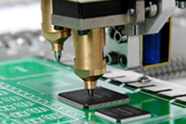
If the PCB passes these tests, it is ready for the next stage—component assembly.