Table of Contents
What is LDO?
LDO (Low Dropout Regulator) is a low dropout linear regulator. Its core features are low voltage drop, linear working mode, and voltage stabilization function. The main function of LDO is to stabilize the input voltage at a fixed output voltage, which is commonly used in portable electronic products. It is widely welcomed due to its simple structure, low cost, and low noise.
How does LDO work?
The working principle of LDO is based on a negative feedback regulation mechanism. Its internal components mainly include a reference voltage source, an error amplifier, a voltage divider sampling resistor, and adjustment elements (usually MOSFETs or transistors).
When the output voltage changes due to load changes, the voltage divider sampling resistor will feedback this change to the error amplifier. The error amplifier compares the output voltage with the reference voltage, adjusts the conduction state of the adjustment component, and stabilizes the output voltage.
I. Typical application of LDO
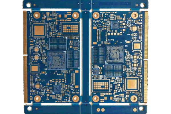
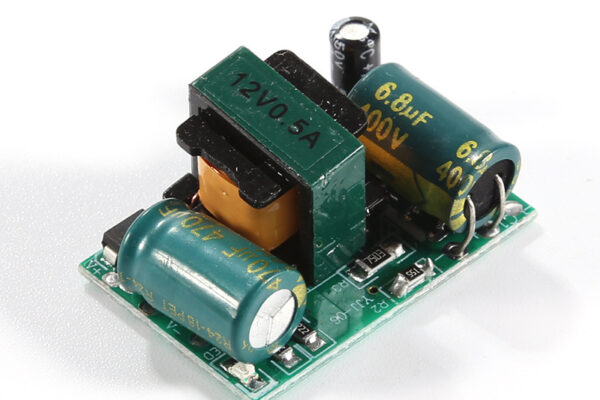
Low dropout voltage regulator, referred to as LDO, compared with traditional linear regulators, is characterized by a voltage drop of one hundred to several hundred mV, or even lower. Below is a typical application circuit diagram.
II. Key parameters and applications of LDO
2.1 voltage drop
Definition of voltage drop: The minimum difference between Vin and Vout required for normal regulation.
Design points:
The minimum difference value. There should be enough design margin in application, and the influence of temperature, load, device parameter discreteness, input voltage accuracy, etc. should be fully considered.
2.2 Input and output capacitors
Below table lists the advantages and disadvantages of the three most common capacitors.
| Material Of Capacitor | Advantages | Disadvantages |
| Aluminum | Often used as a low-pass filter | Polarized |
| High capacitance | Large size | |
| Equivalent series resistance is large | ||
| Overheating possible | ||
| Limited service life | ||
| Large leakage current | ||
| Tantalum | Small size | Polarized |
| Long lasting | ||
| Small leakage current | ||
| Ceramic | Non-polarized | Limited when choosing large capacitors |
| Very small size | DC bias derating | |
| Very small ESR value | ||
| Low cost | ||
| Low tolerance | ||
| High thermal stability |
Design Points for capacitors:
The output capacitance value is within the recommended range of the device datasheet; the actual capacitance value should consider tolerance, temperature change, DC bias characteristics of ceramic capacitors, etc.;
The capacitor is placed close to the LDO pin, if it is placed too far and the PCB connection is too thin, it may cause the LDO to work unstable (in practice, the author has encountered a situation where the LDO is burned by connecting the LDO and the electrolytic capacitor with a thin wire);
2.3 Thermal resistance
Generally, the larger the package size, the lower the device thermal resistance. Rθja, Rθjc, Rθjs can be learned from the datasheet
Thermal resistance (junction to ambient, junction to case, junction to heat sink), LDOs that dissipate more power often have heat sinks.
Design Points:
Estimate how much heat-dissipating copper foil is needed on the PCB.
2.4 Quiescent current
Quiescent current is an important indicator for device selection in low-power mode for battery-powered products. Quiescent is defined as an “inactive or sleep state or phase”, and the quiescent current Iq is the current drawn by the system in standby mode and under light or no-load conditions. For example, the quiescent current of TLV758P is 25uA. Quiescent power consumption (current) is also an important indicator of power devices or products, and even involves some energy-saving certification requirements.