Table of Contents
1 Introduction
Proper Printed Circuit Board (PCB) grounding is not merely a technical detail—it is a fundamental pillar of electronic design that directly determines the performance, reliability, and electromagnetic compatibility (EMC) of any electronic device. Inadequate grounding can lead to many issues, including signal integrity problems, increased electromagnetic interference (EMI), and even complete system failure. For PCB designers and manufacturers, mastering grounding techniques is essential for delivering high-quality products that meet stringent global EMC regulations.
This comprehensive guide delves into the critical aspects of PCB grounding design. We will explore various grounding strategies, provide practical techniques for implementation, and discuss how to avoid common pitfalls. Whether you are designing simple single-layer boards or complex multilayer systems, understanding these principles will help you create more robust and reliable electronic products.
2 Understanding PCB Grounding: Basic Concepts
At its core, grounding provides a common reference point for all electrical signals on a PCB, known as the common potential reference point. This reference is crucial for ensuring stable voltage levels, providing a return path for currents, and shielding against electromagnetic interference.
In electronic systems, you will often encounter different ground types, each serving a specific purpose:
* Signal Ground (SGND): The reference point for analog and digital signals.
* Analog Ground (AGND): A dedicated ground for analog circuits, highly sensitive to noise.
* Digital Ground (DGND): A dedicated ground for digital circuits, which are often noisy due to fast switching.
* Power Ground (PGND): The return path for power supplies and high-current circuits.
* Chassis Ground: A physical connection to the equipment’s metal enclosure for safety and shielding.
A poorly designed grounding system can create ground loops, where potential differences between two ground points cause unwanted current flow, introducing noise and interference. Effective grounding aims to minimize ground impedance and provide the shortest possible return paths for currents, thereby reducing these parasitic effects.

3 Types of Grounding Strategies
Choosing the correct grounding strategy is paramount and depends primarily on the operating frequency of your circuit.
| Strategy | Best For | Key Principle | Advantages | Disadvantages |
| Single-Point Grounding | Low-frequency circuits (<1MHz), e.g., audio amplifiers, sensor interfaces. | All ground connections converge at a single “star” point. | Prevents ground loops, simple to implement. | Impractical for high frequencies due to long paths acting as antennas. |
| Multi-Point Grounding | High-frequency circuits (>10MHz), e.g., RF modules, digital processors. | Components are grounded to the nearest low-impedance ground plane using multiple vias. | Minimizes ground impedance and inductance, reducing EMI radiation. | Can create ground loops if not carefully managed in mixed-signal systems. |
| Hybrid Grounding | Mixed-signal systems (1MHz-10MHz), e.g., industrial PLCs, data acquisition systems. | Combines single-point and multi-point techniques, often using bridges (e.g., ferrite beads, capacitors). | Offers benefits of both strategies, isolating noisy and sensitive grounds. | More complex design and layout required. |
Single-Point Grounding is ideal for low-frequency applications (<1MHz) like audio amplifiers and sensor interfaces. It prevents ground loops by ensuring all currents return to a single point, avoiding potential differences between ground connections. However, at higher frequencies, the long traces required can become inductive and act as antennas, radiating noise.
Multi-Point Grounding is essential for high-frequency circuits (>10MHz), such as digital processors and RF modules. Components are connected to the nearest low-impedance ground plane via short traces or vias. This minimizes the impedance and inductance of the return path, which is critical for reducing EMI at high speeds. A dense array of ground vias (often in a grid pattern) is crucial for this strategy’s effectiveness.
Hybrid Grounding combines both approaches and is frequently used in mixed-signal systems. It involves creating separate ground planes for analog and digital sections, which are then connected at a single point to prevent ground loops. This connection can be made directly or with components like ferrite beads (to block high-frequency noise) or capacitors (to provide a high-frequency AC path while maintaining DC separation).
4 Critical PCB Grounding Techniques
Implementing a robust grounding strategy requires attention to several practical techniques.
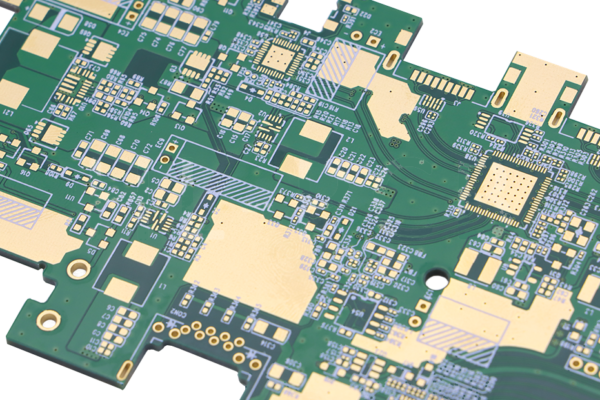
4.1 Ground Planes: The Foundation
A continuous, unbroken ground plane on a dedicated layer is one of the most effective tools for achieving low-impedance grounding. It provides:
* Low impedance return paths for high-frequency signals.
* Natural shielding against EMI, both emitted and received.
* Improved thermal performance through heat dissipation.
To ensure ground plane integrity:
* Avoid Splitting the Plane: If splits are unavoidable (e.g., for isolation), do not route sensitive high-speed signals over the gap.
* Use “Stitching” Vias: Place many ground vias around the perimeter of the board and between different ground regions. This creates a ” Faraday cage ” effect, containing radiation and improving shielding.
* Provide a Good Return Path: Always consider where the return current for a signal will flow. A key rule is to ensure this path is direct and uninterrupted.
4.2 Managing Mixed-Signals: Segmentation and the “Magic Bridge”
Mixed-signal design, where sensitive analog and noisy digital circuits coexist on the same PCB, is a classic challenge.
* Partitioning: Physically separate the analog and digital sections of your board layout.
* Split Ground Planes? The historical approach was to split AGND and DGND planes completely. However, this can create more problems than it solves, as it forces return currents to long, inductive paths, increasing radiation. A more modern approach is “partitioning without splitting”—keeping the ground plane intact but carefully routing signals to avoid cross-talk.
* The Single-Point Connection (“Bridge”): If planes are split, connect them at a single point under or very near the mixed-signal component (e.g., an ADC or DAC). This can be a direct connection, a 0-ohm resistor, a ferrite bead, or a small capacitor, depending on the frequency spectrum of concern.
4.3 Impedance and Current Considerations
•Widen Ground Traces: On layers without a full ground plane, make ground traces as wide as possible—at least 1.5mm (60mil) for single-layer PCBs, and even wider for high-current paths.
•Mind the Current: The ground path must handle the full return current without significant voltage drop. A rule of thumb is to size power and ground traces to handle three times the expected current.
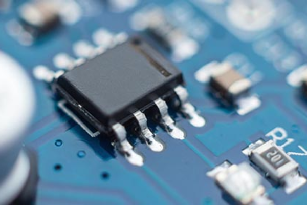
•Use Decoupling Capacitors: Place decoupling capacitors as close as possible between the power pin and ground pin of active ICs. They provide a local, low-impedance source of high-frequency current, shunting noise away from the power and ground planes.
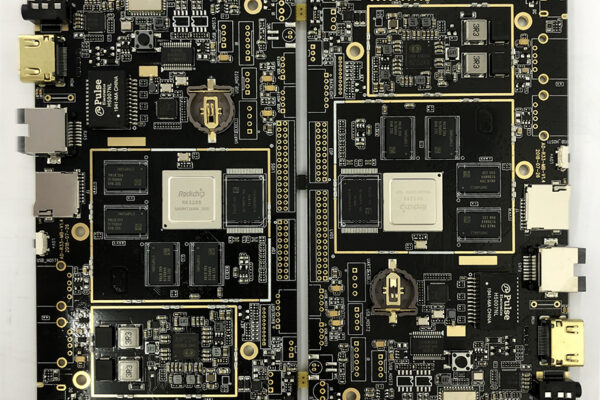
5 Grounding in Multilayer PCBs
Multilayer boards (4+ layers) offer significant advantages for grounding and overall EMC performance.
•Dedicated Ground Layers: A solid internal ground layer is ideal. It provides excellent shielding and a very low-impedance return path for signals on adjacent layers.
•Stack-up Planning: The arrangement of layers is critical. Place the ground layer adjacent to the power layer to form a distributed decoupling capacitor that helps suppress power supply noise. Also, place high-speed signal layers next to ground layers to ensure tight coupling and short return paths.
•Via Placement: Use a generous number of ground vias to connect ground layers together. This minimizes impedance and inductance between layers. Place them near IC ground pins and alongside high-speed signal vias to provide an immediate return path when signals change layers.
6 Handling Mixed-Signal Grounding
The coexistence of analog and digital circuits demands careful grounding to prevent noise from corrupting sensitive analog measurements.
•Partitioning is Key: Physically separate the board into distinct analog and digital zones.
•Grounding Approach: The recommended approach is to use a single, unified ground plane for the entire board. The physical separation of components naturally encourages return currents to flow in their respective areas without the added impedance of a complete physical split.
•Bridge with Care: If you must split the planes, connect them only at a single point, typically beneath the mixed-signal IC. This prevents large digital return currents from flowing through the analog ground section.
•Component Placement: Never place digital components in the analog zone or vice versa. Route all digital signals over the digital section of the ground plane and all analog signals over the analog section.

7 Advanced Techniques and Future Trends
As board densities increase and signals speeds get faster, grounding continues to evolve.
•Simulation-Driven Design: Using electromagnetic simulation tools (like HFSS or CST) early in the design process allows engineers to model power delivery network (PDN) impedance, predict ground bounce, and identify potential EMI issues before fabrication.
•Advanced Materials: The use of flexible materials and novel composites is emerging, which can further enhance grounding performance and reduce EMI in future applications.
•3D Packaging and Integrated Passives: Trends like System-in-Package (SiP) and integrated passive devices move decoupling capacitors and other components inside the package or chip, drastically reducing the loop area and inductance of critical paths, which simplifies board-level grounding challenges.
8 Conclusion
Effective PCB grounding design is a complex but critical discipline that balances fundamental electrical principles with practical layout constraints. There is no one-size-fits-all solution; the optimal approach depends on your circuit’s frequency, functionality, and performance requirements.
The most successful designs prioritize a low-impedance ground system, carefully manage return current paths, and employ strategic segmentation for mixed-signal systems. By adhering to the guidelines outlined in this article—utilizing continuous ground planes, implementing appropriate single-point or multi-point grounding, and leveraging the power of multilayer stack-ups—you can significantly enhance the signal integrity, thermal performance, and EMC robustness of your PCB designs.
As electronics continue to advance, staying informed on simulation tools and emerging materials will be key to mastering the future challenges of PCB grounding.
Partner with Us for Your Next PCB Project
Achieving optimal grounding design requires expertise and precision manufacturing capabilities. Our advanced multilayer PCB fabrication services, support for HDI designs, and strict adherence to international quality standards ensure that your careful designs are translated into reliable, high-performance physical boards.
Contact us today to discuss how we can support your next project and help you build a solid foundation for your electronic products.