Table of Contents
Executive Summary
Via technologies represent one of the most critical aspects of modern printed circuit board design and manufacturing, enabling the three-dimensional interconnection that powers today’s sophisticated electronics. From traditional through-hole vias to advanced through-silicon vias (TSV), through-plastic vias (TPV), and through-glass vias (TGV), each technology offers unique advantages for specific applications ranging from consumer electronics to high-performance computing and medical devices. This comprehensive guide explores the technical characteristics, manufacturing processes, applications, and comparative advantages of these four fundamental via technologies, providing PCB designers and engineers with essential knowledge for selecting the optimal interconnection strategy for their projects.
1.Introduction to Via Technologies in PCB Manufacturing
Vias are fundamental conductive pathways that enable electrical connections between different layers of a printed circuit board or integrated circuit package. As electronic devices continue to evolve toward miniaturization, higher performance, and increased functionality, the importance of advanced via technologies has grown exponentially. These tiny interconnects serve as the vertical highways that carry signals and power through the various layers of modern electronic systems, making them indispensable in today’s multi-layer PCB designs and 3D packaging architectures.
The evolution of via technologies has been driven by several key industry trends: the relentless pursuit of higher component density, the need for improved signal integrity at higher frequencies, demands for enhanced thermal management, and the ongoing push toward heterogeneous integration where multiple technologies are combined in single packages. Understanding the capabilities and limitations of each via type is essential for optimizing PCB designs for performance, reliability, and cost-effectiveness across diverse applications from consumer electronics to aerospace systems.
2.Through-Hole Vias: The Foundation of PCB Interconnection
2.1 Technology Overview and Manufacturing Process
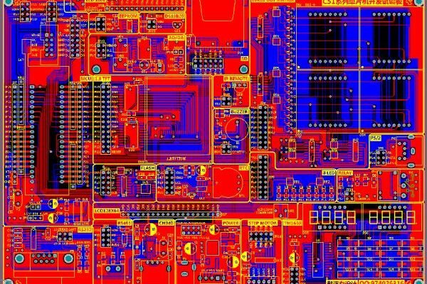
Through-hole vias represent the original and most fundamental via technology in PCB manufacturing. These vias are created by drilling completely through the entire PCB substrate and then plating the hole walls with conductive material, typically copper, to establish electrical connectivity between all layers of the board. The manufacturing process involves several critical steps: drilling (mechanical or laser), desmearing to remove resin residue, electroless copper deposition to make the hole walls conductive, and electrolytic copper plating to build up the required thickness.
The reliability and simplicity of through-hole vias have made them a staple in PCB design for decades. They provide robust mechanical connections and excellent thermal conduction paths, making them particularly valuable in applications requiring high reliability or where thermal management is a concern. However, their consumption of significant board real estate on all layers has driven the development of more space-efficient alternatives for high-density designs.
2.2 Design Considerations and Applications
Through-hole vias present specific design considerations that engineers must address:
•Aspect Ratio Limitations: Traditional drilling technology typically limits the aspect ratio (board thickness to drill diameter) to approximately 10:1 for reliable plating, though advanced processes can achieve higher ratios.
•Annular Ring Requirements: Sufficient copper pad size around the via hole must be maintained to ensure reliable connections and accommodate registration tolerances during manufacturing.
•Signal Integrity: At high frequencies, the stub effect of through-hole vias passing through unused layers can cause signal reflections, potentially necessitating back-drilling in critical applications.
Despite these limitations, through-hole vias remain widely used in many applications including power electronics, industrial control systems, automotive electronics, and other scenarios where mechanical robustness, high current carrying capacity, or superior thermal performance are prioritized over maximum interconnection density.

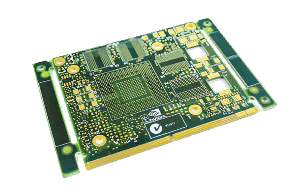
3.Through-Silicon Vias (TSV): Enabling 3D Integration
3.1 Technology Fundamentals
Through-silicon vias (TSV) represent a revolutionary advancement in interconnection technology that enables vertical integration of multiple silicon dies in a three-dimensional stack. Unlike traditional interconnections that use wire bonding or flip-chip connections at the periphery of chips, TSVs create direct vertical pathways through the silicon substrate itself, dramatically reducing interconnection length and improving electrical performance.
The TSV manufacturing process involves several sophisticated steps: deep reactive ion etching (DRIE) to create high-aspect-ratio holes in silicon, dielectric layer deposition for electrical isolation, barrier and seed layer deposition, copper electroplating to fill the vias, and chemical-mechanical polishing (CMP) to planarize the surface. This process flow enables the creation of vias with diameters as small as 1-5μm and aspect ratios exceeding 10:1, facilitating extremely high interconnection densities unmatched by other technologies.
3.2 Applications and Implementation Variants
TSV technology has become foundational to several advanced packaging approaches:
•3D Stacked Memory: High-bandwidth memory (HBM) and hybrid memory cube (HMC) architectures use TSVs to vertically stack multiple memory dies, dramatically increasing bandwidth while reducing footprint.
•Image Sensors: CMOS image sensors extensively use TSVs to route connections to the backside of the sensor, enabling smaller pixel sizes and higher fill factors.
•Heterogeneous Integration: TSVs enable the combination of disparate technologies (logic, memory, RF, etc.) in a single 3D stack, optimizing performance and power efficiency for specific applications.
TSV implementation occurs at different stages of device fabrication: via-first (before transistor formation), via-middle (after transistors but before metallization), and via-last (after complete device fabrication), each approach offering distinct advantages for specific applications and device types.
4.Through-Plastic Vias (TPV): Flexible Circuit Solutions
4.1 Technology Characteristics
Through-plastic vias (TPV) represent a specialized via technology designed for interconnection through polymer substrates, particularly in flexible printed circuits (FPCs) and rigid-flex PCB applications. Unlike the rigid materials used in conventional PCBs and silicon interposers, plastic substrates present unique challenges including lower thermal stability, higher coefficient of thermal expansion (CTE), and different mechanical properties that must be addressed in the via formation process.
TPV manufacturing typically employs laser ablation techniques—often using UV or CO₂ lasers—to create vias in polymer materials such as polyimide, PET, or LCP. The process continues with metallization approaches that may include electroless copper plating, sputtering, or conductive paste filling, depending on the specific application requirements and material compatibility. The lower processing temperatures required for plastic substrates represent a key differentiator from via technologies used with high-temperature materials.
4.2 Applications and Advantages
TPV technology enables several important applications:
•Flexible and Wearable Electronics: TPVs provide reliable interconnections in bendable circuits for wearable devices, medical sensors, and flexible displays.
•High-Density Interconnects: In advanced packaging, TPVs enable fine-pitch connections in organic interposers that bridge the gap between conventional PCBs and silicon interposers.
•Rigid-Flex PCBs: TPVs facilitate connections between rigid and flexible sections in complex multilayer assemblies used in aerospace, medical, and consumer electronics.
The key advantages of TPV technology include lower cost compared to TSVs, compatibility with large-panel processing, and mechanical flexibility that enables innovative form factors not possible with rigid substrate technologies.

5.Through-Glass Vias (TGV): RF and MEMS Applications
5.1 Technology Overview
Through-glass vias (TGV) represent an emerging via technology that leverages the exceptional electrical and mechanical properties of glass substrates for advanced applications, particularly in radio frequency (RF) systems and micro-electromechanical systems (MEMS). Glass offers several advantageous properties including excellent high-frequency characteristics, tailorable coefficient of thermal expansion (CTE), superior dimensional stability, and optical transparency that enable unique functionality.
TGV fabrication typically employs one of two primary approaches: laser-assisted etching where laser modification of the glass structure enables selective chemical etching, or powder blasting for larger via structures. Following via formation, metallization is achieved through processes such as copper electroplating, silver paste filling, or copper direct plating on specially treated glass surfaces. The inherently insulating nature of glass eliminates the need for additional dielectric layers, simplifying the manufacturing process compared to TSVs.
5.2 Applications and Performance Advantages
TGV technology enables several high-performance applications:
•RF and Millimeter-Wave Devices: The low electrical loss and consistent dielectric properties of glass make TGVs ideal for 5G/6G communications, automotive radar, and satellite systems where signal integrity at high frequencies is critical.
•MEMS and Sensor Packaging: Glass substrates with TGVs provide hermetic encapsulation for sensitive MEMS devices while enabling electrical interconnections, particularly in inertial sensors, microphones, and environmental sensors.
•Advanced Display Interposers: The optical transparency of glass enables TGV-based interposers for high-resolution displays where interconnections cannot obstruct the active display area.
•Photonic Integration: TGVs facilitate electrical connections in photonic integrated circuits while maintaining optical access paths through the transparent substrate.
The performance advantages of TGV technology include superior high-frequency performance with insertion losses potentially 50% lower than silicon-based interposers, enhanced thermal stability for high-temperature applications, and the ability to create ultra-fine pitch interconnections with via densities exceeding 10,000 vias/mm² in advanced implementations.
6.Comparative Analysis: Key Parameters and Selection Criteria
6.1 Technical Performance Comparison
Table: Comparative Analysis of Via Technologies
| Parameter | Through-Hole Via | TSV | TPV | TGV |
| Typical Diameter | 100-500 μm | 1-20 μm | 20-100 μm | 10-100 μm |
| Aspect Ratio | Up to 10:1 | 5:1 to 20:1 | 1:1 to 5:1 | 2:1 to 10:1 |
| Substrate Material | FR-4, Ceramics | Silicon | Polymers (PI, LCP) | Glass |
| Process Temperature | High (>200°C) | Very High (>400°C) | Low-Medium (<200°C) | Medium (200-400°C) |
| Relative Cost | Low | High | Medium | Medium-High |
| Signal Integrity | Good (with back-drill) | Excellent | Good | Exceptional (RF) |
| Thermal Conductivity | Good | Excellent | Poor | Poor |
| CTE Match to Si | Poor | Excellent | Poor | Excellent (tailorable) |
| Key Applications | Standard PCBs, Power | 3D ICs, Memory | Flexible Circuits, HD Interposers | RF, MEMS, Photonics |
6.2 Selection Guidelines for PCB Designers
Choosing the appropriate via technology requires careful consideration of multiple factors:
•Performance Requirements: For high-frequency applications above 10GHz, TGV technology typically provides superior performance, while TSV offers the highest density for 3D integration.
•Thermal Management Needs: Applications with significant power dissipation may benefit from through-hole vias or TSVs due to their superior thermal conduction properties.
•Mechanical Constraints: Flexible or bendable applications necessitate TPV technology, while systems requiring exceptional dimensional stability may benefit from TGV or TSV approaches.
•Cost Considerations: Through-hole vias remain the most cost-effective solution for standard applications, while TSV technology commands a premium justified only in highest-performance applications.
•Manufacturing Complexity: Designers must consider the manufacturing infrastructure required for each technology, with through-hole vias being universally available while specialized technologies like TSV and TGV require dedicated fabrication facilities.
7.Future Trends and Developments in Via Technologies
The evolution of via technologies continues to address emerging challenges in electronics packaging:
•Heterogeneous Integration: Advanced via technologies will increasingly enable the combination of disparate technologies (logic, memory, analog, RF) in single packages, with TSV and TGV playing pivotal roles.
•Further Miniaturization: The drive toward smaller via dimensions continues, with research focused on sub-micron TSVs and ultra-fine-pitch TGVs to support next-generation 3D integration.
•Advanced Materials: New substrate materials and metallization approaches are under development to enhance performance, with particular focus on low-loss polymers for TPVs and specialized glass formulations for TGVs.
•Thermal Management Integration: Future via technologies will increasingly incorporate dedicated thermal management features, including integrated microfluidic cooling channels in 3D stacks.
•Additive Manufacturing Approaches: Emerging printing and additive techniques may complement traditional via formation methods, particularly for TPVs and specialized applications.
8.Conclusion
Via technologies form the critical vertical interconnection pathways that enable the three-dimensional integration essential to modern electronics. Each technology—through-hole vias, through-silicon vias (TSV), through-plastic vias (TPV), and through-glass vias (TGV)—offers unique advantages tailored to specific applications, materials, and performance requirements.
For PCB designers and engineers, selecting the optimal via technology requires careful consideration of electrical performance, thermal management, mechanical constraints, and cost targets. As electronic systems continue to evolve toward higher frequencies, greater integration densities, and more specialized applications, the strategic implementation of advanced via technologies will become increasingly critical to achieving system-level performance goals.
The ongoing development of via technologies will continue to push the boundaries of what’s possible in electronic packaging, enabling new generations of smaller, faster, and more capable electronic systems across consumer, automotive, aerospace, and computing applications.
Partner with Us for Your Advanced PCB Requirements
Our expertise in advanced PCB manufacturing encompasses all via technologies, from traditional through-hole vias to cutting-edge TSV, TPV, and TGV implementations. We provide comprehensive design support and manufacturing capabilities to help you select and implement the optimal via strategy for your specific application requirements.
Contact us today to discuss how our via technology expertise can enhance the performance, reliability, and miniaturization of your next PCB project.