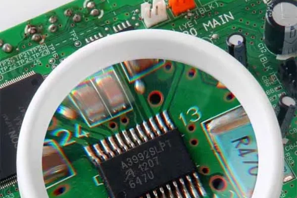
In the field of Industrial Internet of Things (IIoT) and Machine to Machine (M2M) communication, PCB serves as the core carrier of electronic devices, and the selection of its laminated board directly affects the reliability, signal integrity, and long-term stability of the equipment. This article will provide key guidance for PCB design in M2M applications from the perspectives of material properties, stack design, and cost optimization.
Table of Contents
1、 Core requirements for M2M design and key points for selecting laminates
M2M devices are typically deployed in complex environments such as high temperature, high humidity, vibration, etc. Therefore, PCB laminates need to meet the following requirements:
1. High reliability: excellent mechanical strength, heat resistance (such as high glass transition temperature Tg) and aging resistance are required.
2. Signal integrity: High frequency communication scenarios (such as 5G modules) require materials with low dielectric constant (Dk) and loss tangent (Df) to reduce signal attenuation.
3. Environmental adaptability: It is necessary to consider the compatibility of coefficient of thermal expansion (CTE) to avoid delamination or connection failure caused by temperature changes.
4. Cost effectiveness: Balancing material costs and manufacturing process complexity while ensuring performance.
2、 Common PCB laminate materials and their applicable scenarios
1. FR-4 epoxy resin substrate
-Features: Low cost, high mechanical strength, flame resistance in accordance with UL94V0 standard, suitable for universal M2M devices.
-Limitations: High dielectric loss (Df ≈ 0.02), not suitable for high-frequency signal transmission above 10 GHz.

2. Polyimide (PI) substrate
-Characteristics: High temperature resistance (Tg>250 ° C), strong chemical stability, suitable for high-temperature industrial environments or aerospace equipment.
-Cost considerations: High price, recommended for use in critical components or extreme environments.
3. High speed and low loss materials (such as Megtron 6, Rogers 4350B)
-Features: Dk ≈ 3.4, Df<0.003, suitable for high-speed communication modules (such as 28 Gbps and above), significantly reducing signal attenuation.
4. Metal substrate (aluminum/copper based)
-Features: Excellent heat dissipation performance, suitable for high-power M2M devices (such as power management modules), can improve device lifespan.
3、 Best practices for stacked design
1. Layered planning:
-The 4-8 layer board is a common choice for M2M design, depending on the signal complexity. For example, it is recommended to use a stripline layout for high-speed signals to enhance isolation.
-The power and ground layers should be arranged adjacent to each other to reduce impedance and electromagnetic interference.

2. Blind hole and buried hole technology:
-In high-density design, using blind holes or buried holes can save wiring space, but the process cost needs to be balanced.
3. Impedance control:
-To achieve the target impedance (such as 50 Ω differential pair) by adjusting the line width and dielectric layer thickness, simulation needs to be conducted in conjunction with the material Dk value.
4、 Cost optimization strategy
1. Classification of board selection:
-TG130 board is used in ordinary scenarios, and TG150 or TG170 is selected for multi-layer boards (6 layers or more) to enhance heat resistance and avoid excessive pursuit of high specifications.
2. Splicing design and process simplification:
-By optimizing the layout of the splicing board, the utilization rate of the board can be improved and the waste of corner materials can be reduced.
-Avoid unnecessary customization processes (such as ultra-thin copper foil) and choose commonly used specifications from board manufacturers to reduce processing difficulty.
3. DFM (Design for Manufacturability) tool application:
-Use DFM software to analyze design risks (such as insufficient line spacing and inconsistent aperture) and reduce trial and error costs.
5、 Summary
In the design of M2M devices, the selection of PCB laminates should comprehensively consider performance, environmental adaptability, and economy. For example, industrial sensors can use FR-4 substrates to control costs, while high-frequency communication modules need to be paired with low loss materials such as Megtron 6. Meanwhile, through scientific stacking design and DFM optimization, cost reduction and efficiency improvement can be achieved while ensuring reliability.
As a professional PCB manufacturer, we provide full process support from material selection to stack design, helping customers create high-performance and cost-effective M2M solutions. If you need further consultation or case references, please feel free to contact our technical team.