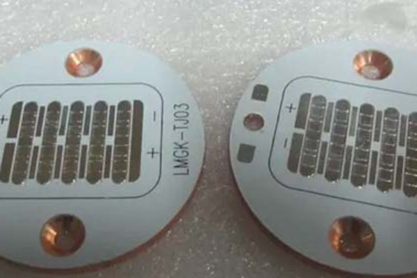
PCB silkscreen plays a critical role in ensuring proper assembly, troubleshooting, and maintenance of printed circuit boards (PCBs). It provides textual and symbolic information, such as component identifiers, pin numbers, logos, and warnings, which aid manufacturers and engineers. However, designing an effective PCB silkscreen requires careful consideration of several key details to ensure clarity, accuracy, and manufacturability.
What are the key details of PCB silkscreen?
1. Component Labeling
Proper labeling of components is essential for assembly and debugging processes. Here are some tips:
Unique Identifiers: Each component should have a unique reference designator (e.g., R1, C1, U1) to avoid confusion.
Readable Fonts: Use legible font sizes that are not too small. A minimum height of 0.8 mm is typically recommended.
Placement: Place labels near their corresponding components without obstructing solder pads or vias. Ensure that labels remain visible even after assembly.
2. Alignment and Orientation
Consistency in alignment and orientation enhances the readability of the silkscreen:
Uniform Direction: Align text and symbols in a consistent orientation, usually readable from the bottom or right side of the PCB.
Grid Alignment: Adhere to a grid system to maintain order and neatness in label placement.
3. Avoid Overlapping Critical Areas
Silkscreen should not interfere with critical PCB features:
Pads and Holes: Ensure no silkscreen markings are placed on solder pads, vias, or through-holes to avoid issues during soldering.
Edge Clearance: Maintain adequate clearance from the edges of the PCB to prevent silkscreen distortion during fabrication.
4. Color and Contrast
Silkscreen visibility depends on the color contrast between the markings and the PCB:
Standard Colors: White silkscreen on green solder mask is the most common combination. Other contrasting combinations, such as yellow on black, can be used based on design requirements.
Avoid Overcrowding: Ensure sufficient spacing between silkscreen elements to enhance readability.
5. Inclusion of Key Information
The silkscreen should provide essential information for various stakeholders:
Company Logo and PCB Version: Include the company’s logo and PCB version number for identification.
Warnings and Polarity Markings: Use standard symbols and warnings (e.g., polarity indicators for capacitors and diodes) to guide assembly.
Testing Points: Clearly label test points for easier debugging and quality control.
6. Manufacturing Guidelines
Silkscreen design must adhere to the capabilities of the PCB manufacturer:
Minimum Line Width and Text Size: Verify the minimum line width and text size supported by your manufacturer. Typically, a line width of 0.15 mm and a text height of 1.0 mm are recommended.
Layer Considerations: Place silkscreen on the component side (top layer) unless additional markings are required on the bottom side.
DFM Checks: Run design-for-manufacturability (DFM) checks to ensure the silkscreen meets fabrication constraints.
7. Use of Software Tools
Modern PCB design software offers tools to streamline silkscreen design:
Layer Management: Use dedicated silkscreen layers to prevent accidental interference with copper or solder mask layers.
Clarity Verification: Preview the silkscreen in a 3D viewer to confirm its clarity and placement.
Auto-Placement Features: Leverage auto-placement features while manually fine-tuning critical labels.
Conclusion
A well-designed PCB silkscreen significantly contributes to the manufacturability, usability, and maintainability of the PCB. By adhering to best practices in component labeling, alignment, manufacturing guidelines, and using the right tools, designers can create clear, professional silkscreen layouts that benefit all stakeholders. Always collaborate with your PCB manufacturer to ensure your design aligns with their fabrication capabilities.