In the relentless drive towards smaller, faster, and more powerful electronic devices, Printed Circuit Board (PCB) design and manufacturing face constant challenges. One critical process enabling this miniaturization and performance leap is Via Filling. At [Your Company Name], we leverage advanced via filling technologies to deliver PCBs that meet the demanding requirements of today’s sophisticated electronics.
Table of Contents
What is a Via and Why Fill It?
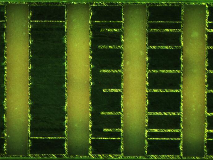
A via is a small hole drilled through a PCB layer (or layers) to electrically connect traces on different levels. While essential for multi-layer boards, traditional unfilled or tented vias present limitations:
•Trapped Contaminants: Open vias can trap process chemicals during plating and cleaning, leading to potential reliability issues like corrosion or dendrite growth.
•Weak Solder Joints: During assembly, solder can wick down unfilled vias (especially on BGA pads), starving the joint and causing weak connections or opens.
•Signal Integrity Issues: Stub effects from long, unused via barrels can degrade high-speed signals.
•Planarity Challenges: Unfilled vias create surface unevenness, making it difficult to place fine-pitch components accurately.
•Thermal Stress: Air trapped in vias expands during soldering, potentially causing delamination (popcorning).
Via filling addresses these challenges by completely or partially filling the via hole with a specialized material, transforming it from a potential liability into an asset.
Types of Via Filling Technologies
We offer tailored via filling solutions to meet diverse application needs:
1.Conductive Epoxy Filling:
–Material: Filled with electrically conductive epoxy (often silver-filled).
–Key Benefit: Creates a continuous thermal and electrical path through the via barrel.
–Applications: Essential for thermal vias under high-power components (LEDs, processors), grounding vias requiring low impedance, or when the filled via is used as a surface mount pad (VIPPO – Via-in-Pad Plated Over). Maximizes heat dissipation and electrical connectivity.
2.Non-Conductive Epoxy/Resin Filling:
–Material: Filled with insulating epoxy or resin.
–Key Benefit: Provides excellent surface planarity, prevents solder wicking, seals the via against contaminants, and improves reliability.
–Applications: Ideal for via-in-pad designs (where a component sits directly over the via) to prevent solder escape and ensure coplanarity. Crucial for HDI boards, fine-pitch BGAs, and applications demanding high reliability in harsh environments. Also used for plugging via entrances (“capping”) before surface finishing.
3.Copper Plating Filling (Electrolytic Copper):
–Process: Via holes are completely filled with solid copper using specialized electroplating processes.
–Key Benefit: Offers the ultimate in electrical and thermal conductivity through the via. Provides superior mechanical strength and eliminates any chance of voids or outgassing.
–Applications: Highest-end applications requiring maximum thermal management (power electronics, RF), ultra-high reliability (military, aerospace, medical), and the best possible signal integrity for very high-speed designs.
Key Advantages of Using Via Filling from SysPCB
•Enhanced Reliability: Eliminates contamination traps, prevents solder wicking, reduces risk of thermal-mechanical failure (popcorning), and strengthens the via structure.
•Improved Signal Integrity: Minimizes stub effects and impedance discontinuities, critical for high-speed digital and RF circuits.
•Superior Thermal Management: Conductive fills (especially copper) provide efficient heat transfer paths away from hot components, improving performance and lifespan.
•Increased Design Density & Miniaturization: Enables Via-in-Pad (VIP) technology, allowing components to be placed directly over vias. This is fundamental for High-Density Interconnect (HDI) PCBs and miniaturized devices.
•Improved Surface Planarity: Creates a flat surface essential for the accurate placement and soldering of fine-pitch components like BGAs, QFNs, and 01005 chips.
•Better Solder Joint Quality: Prevents solder starvation on BGA/CSP pads containing vias.
•Stronger Mechanical Structure: Filled vias add rigidity to the PCB stackup.
Applications Demanding Via Filling
Via filling is no longer just a premium option; it’s becoming essential for many cutting-edge applications:
•High-Density Interconnect (HDI) PCBs: Essential for smartphones, tablets, wearables.
•Ball Grid Array (BGA) & Chip Scale Package (CSP): Especially with via-in-pad designs.
•High-Speed Digital Design: Servers, networking equipment, high-speed computing.
•RF & Microwave Circuits: Radar, communication systems.
•Power Electronics: LED lighting, power supplies, motor drives (thermal management).
•Automotive Electronics: Engine control units (ECUs), ADAS systems (reliability in harsh environments).
•Aerospace & Defense: Avionics, mission-critical systems.
•Medical Devices: Implantable devices, diagnostic equipment.
SysPCB: Your Expert Partner in Advanced Via Filling
Choosing the right via filling technology requires deep expertise and precision manufacturing capabilities. At [Your Company Name], we combine:
•Advanced Technology: State-of-the-art filling lines for conductive epoxy, non-conductive resin, and copper plating processes.
•Stringent Process Control: Rigorous control over material preparation, filling, curing, and planarization (leveling) to ensure void-free fills, perfect surface flatness, and consistent results.
•Material Expertise: We select high-performance, reliable filling materials suited to your specific electrical, thermal, and environmental requirements.
•IPC Standards Compliance: Our processes adhere strictly to relevant IPC standards (e.g., IPC-4761 for via protection) for guaranteed quality.
•Design for Manufacturability (DFM) Support: Our engineering team works closely with your designers to optimize via placement, size, and filling strategy for manufacturability, performance, and cost-effectiveness.
Conclusion
Via filling is a sophisticated but increasingly necessary process in modern PCB manufacturing. It solves critical challenges related to reliability, miniaturization, thermal management, and signal performance. By partnering with SysPCB, you gain access to expert via filling capabilities that ensure your PCBs meet the highest standards of quality and performance for the most demanding applications.
Get your exclusive quote immediately: fill out the form or send an email directly.As a professional PCB manufacturer for hobbyist , we will provide you with a quote service within 24 hours. Enjoy free DFM optimization and a 10% discount on SMT patches for your first order!