Table of Contents
Introduction
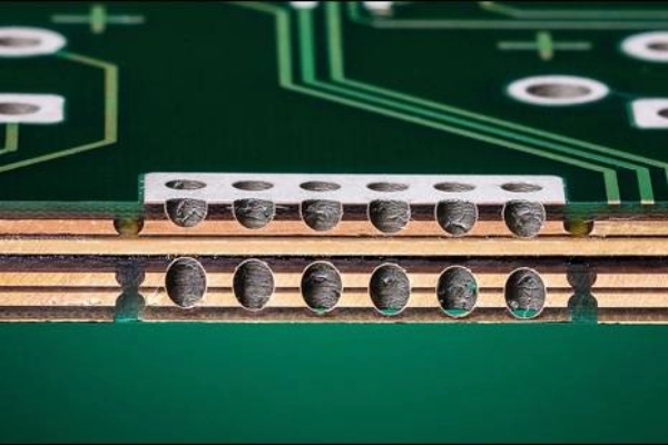
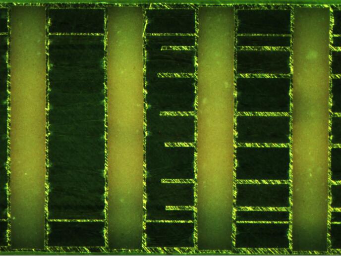
Resin plugging (via filling) is a pivotal process in modern PCB manufacturing, enabling higher circuit density, improved signal integrity, and enhanced reliability for demanding applications like 5G communications, HDI boards, and automotive electronics. As components shrink and data speeds soar, this technology addresses critical challenges such as solder wicking, thermal stress, and signal loss. Here’s how advanced resin plugging elevates PCB performance .
Ⅰ.Why Resin Plugging Matters
Unfilled vias pose significant risks:
– Solder Wicking: Solder drains into hollow vias during assembly, causing weak joints (especially under BGAs) .
– Signal Degradation: Unfilled “stubs” in back-drilled vias distort high-frequency signals .
– Contamination & Corrosion: Trapped chemicals or moisture lead to dendritic growth and failures .
– Thermal Stress: Air expansion in vias during soldering causes delamination (“popcorning”) .
Resin plugging eliminates these issues by sealing vias with thermally stable, conductive/non-conductive materials.
Ⅱ.Key Applications & Technologies
1. POFV (Plating Over Filled Via) for Via-in-Pad (VIP)
- Process: Vias are drilled → plated → resin-filled → planarized → plated over to create flat solderable pads .
- Advantages: Enables direct component placement over vias, reducing board size and layer count. Critical for HDI designs in smartphones and wearables .
2. Back-Drilling with Resin Filling
- Purpose: Removes unused copper “stubs” in high-speed vias to minimize signal loss.
- Challenge: Resin-copper separation due to mismatched thermal expansion coefficients (e.g., PTFE vs. FR-4) .
- Solution: Material compatibility testing and low-expansion resins (e.g., modified epoxies) .
3. Inner-Layer Buried Via Filling
- Ensures uniform dielectric thickness during lamination, preventing voids and delamination in multilayer boards .
Ⅲ.Overcoming Critical Challenges
– Cracking in High Aspect-Ratio (AR) Vias
- Cause: Stress from resin shrinkage during curing in AR > 10:1 vias .
- Solution: Optimized resin formulas (e.g., silica-filled epoxies) and staged curing protocols .
– Poor Copper Adhesion in POFV
- Cause: Standard resins carry negative charges, repelling colloidal palladium catalysts during electroless copper plating .
- Breakthrough: Modified cationic resins (e.g., SKY-2000 I-3) incorporate positive-charge additives (e.g., sulfonated triazine-cazole), improving Pd adsorption and copper coverage .
– Resin-Copper Separation in Back-Drilling
- Root Cause: Differential expansion between resin and high-Tg laminates (e.g., PTFE) .
- Fix: Material pairing with matched CTE and low-hardness resins (e.g., 1H vs. traditional 8H) to reduce grinding stress .
Ⅳ.Material Innovations Driving Reliability
| Resin Type | Key Properties | Applications |
| Conductive Epoxy | Silver-filled; thermal/electrical continuity | VIPs under high-power ICs, LEDs |
| Non-Conductive | Low CTE, high planarization | HDI, fine-pitch BGAs, harsh environments |
| Modified Epoxies | Cationic polarity; void-free filling | POFV processes; high-reliability boards |
| PTFE-Based | Ultra-low Dk/Df; enhanced thermal stability | 5G/mmWave RF PCBs |
Table 1: Advanced resins for specialized plugging needs .
Ⅴ.Design & Cost Optimization Tips
- Avoid Mixed Plugging: Combining resin and solder-mask filling in one design increases costs and defects. Unified POFV is preferred .
- Aspect Ratio Limits: For reliable filling:
- Max via diameter: 0.6mm
- Max board thickness: 3.2mm (solder-mask fill) / 2.4mm (resin fill) .
- Cost Insight: POFV pricing depends on process steps, not via count. Full-board resin plugging often costs less than partial treatments .
Ⅵ.The Future: Resin Plugging in 5G & Beyond
- Low-Loss Materials: PTFE and ceramic-filled resins dominate 5G PCBs, reducing signal attenuation at mmWave frequencies .
- Thermal Management: Conductive fills (copper/epoxy) dissipate heat from high-power ICs in data centers .
- Supply Chain Shifts: Domestic production of high-end resins (e.g., CE, PPE) is rising to replace imports, driven by 5G demands .
Why Choose SysPCB for Resin Plugging?
- Expertise: Precision control of filling, curing, and planarization for void-free results.
- Advanced Solutions: Cationic resins for robust POFV, CTE-matched materials for back-drilling.
- Quality Compliance: Adherence to IPC-4761 (Type VII “Filled and Capped”) standards .
- DFM Support: Collaborative design reviews to optimize via placement, AR, and material selection.
Unlock higher density, reliability, and signal performance with our resin plugging solutions. [Contact SysPCB for a quote or technical consultation].