As the intersection of semiconductor technology and high-frequency circuits, Varactor diode have become the core components of modern wireless communication, RF tuning, and signal processing by regulating the capacitance characteristics through voltage. The deep synergy between it and PCB design directly determines the performance boundary and reliability limit of high-frequency circuits. This article will delve into the working principle, design challenges, and future trends of varactor diodes, providing key technical guidance for electronic engineers.
Table of Contents
1、 Physical Essence: Quantum Game of Voltage and Capacitance
The core of a varactor diode is to utilize the depletion layer effect under PN junction reverse bias to achieve dynamic capacitance regulation:
-Depletion layer regulation mechanism:
-Reverse voltage increases → depletion layer widens → capacitance decreases ($C=\ frac {\ epsilon \ cdot S} {d} $, $d $is the depletion layer width)
-Reverse voltage decreases → depletion layer narrows → capacitance increases
-Nonlinear response: The rate of change of capacitance is exponentially related to voltage and needs to be compensated through circuit linearization
Material Evolution Path:
-Silicon (Si): Low cost, mature process, suitable for conventional RF circuits ≤ 3GHz
-Gallium Arsenide (GaAs): High electron mobility, supports millimeter wave frequency band (>30GHz), Q value increased by 40%
2、 Varactor diode–Key parameters: The golden standard for selection and design
1. Core performance indicators
| Parameters | Definition | Design Impact | Typical Value Range |
| Zero bias junction capacitance (Cj0) | Initial capacitance at zero voltage | Determine fundamental resonant frequency | 2-100 pF |
| Capacitance ratio (Cmax/Cmin) | Maximum to minimum capacitance ratio | Tuning range width | 1.5:1 – 20:1 |
| Reverse breakdown voltage (Vr) | Maximum withstand reverse voltage | Safe operating voltage threshold | 15-50 V |
| Q value (quality factor) | energy storage to energy consumption ratio | high-frequency circuit signal loss | 100-3000 @ 1GHz |
2. Collaborative adaptation of packaging technology
-Surface mount packaging (SOT-23/SOD-323):
-Suitable for high-frequency circuits below 10GHz, parasitic inductance<1nH
-Automatic mounting accuracy ± 0.02mm, improving SMT yield
-Glass sealed packaging:
-Strong corrosion resistance, passed the 150 ℃/1000 hour salt spray test
-Essential for Automotive Electronics and Industrial Environment
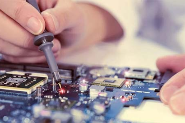
3、 Five Practical Challenges in PCB Design
1. Bias noise suppression
-Adopting a π – type filtering network (10nF MLCC+1 μ F tantalum capacitor), ripple suppression>60dB
-Bias voltage routing with ground wrapping treatment, spacing ≤ 0.2mm to prevent crosstalk
2. High frequency layout optimization

-Shortest path rule: If the distance between the varactor diode and the VCO chip is less than 5mm, reduce the path inductance
-Microstrip line impedance matching: The impedance line width of 50 Ω needs to be accurately calculated based on the substrate Dk value (such as Dk=4.5 for FR-4, line width ≈ 2.9mm for 1.6mm plate thickness)
3. Temperature drift compensation
-Negative temperature coefficient varactor diode (such as BBY52 series) paired with NTC thermistor
-Copper foil heat dissipation island design, temperature rise controlled within Δ T < 10 ℃
4. Grounding strategy
-Independent ground plane segmentation to avoid coupling of digital noise
-Grounding via array (aperture 0.3mm/spacing 1.0mm), reducing ground impedance by 30%
5. Anti static design
-Series connected 330 Ω resistor for current limiting, parallel TVS tube for absorbing ESD pulses
-Solder mask windows should avoid high voltage pins, and the creepage distance should be ≥ 0.5mm
4、 Frontier Applications: From 5G to Quantum Communication
1. Millimeter wave phased array antenna
-In 28GHz 5G base stations, varactor diodes achieve microsecond level switching of beam pointing
-Integrated on AiP (antenna package) substrate, capacitance adjustment accuracy ± 0.1pF
2. Flexible wearable devices
-Polymer based varactor diode (bending radius>5mm)
-Textile circuit integration, supporting dynamic frequency modulation of human body sensing network
3. Quantum Bit Control
-GaAs varactor diode regulates quantum dot energy levels in ultra-low temperature (4K) environment
-Capacitor voltage linearity error<0.05%, ensuring quantum state stability
5、 Manufacturing Trends: Intelligence and Heterogeneous Integration
-AI assisted tuning:
Dynamically adjust bias voltage based on real-time impedance monitoring data, with a response speed of less than 10 μ s
-3D stacked packaging:
The varactor diode is embedded in the inner layer of the PCB and vertically interconnected with the silicon transfer board, reducing the size by 60%
Conclusion: Reshaping the Connection at the Boundary of Voltage and Frequency
The essence of varactor diodes lies in converting the silent changes in voltage into precise frequency transitions – from the manual knobs of radios to the intelligent beams of 5G base stations, this nanoscale physical effect continues to drive the revolution of communication technology.
>Nobel laureate in Physics Herbert Kramer once asserted:
>The greatness of semiconductor devices lies in taming the chaos of the electromagnetic world with the controllability of their microstructure
As a technical team with 20 years of experience in high-frequency PCB manufacturing, we provide full process solutions from variable capacitance diode selection to millimeter wave circuit layout. Whether it is automotive grade AEC-Q200 certified boards or quantum computing ultra-low noise substrates, impedance control ± 3% and dielectric loss ≤ 0.0015 are the standards – because what is more important than signal connectivity is the purity of every decibel in the GHz flood.