Table of Contents
Introduction
Low-Power Wide-Area Network (LPWAN) technology has emerged as a transformative force in the Internet of Things (IoT) landscape, enabling long-range communication with minimal power consumption. For PCB enterprises, understanding LPWAN’s technical nuances and design requirements is essential to capitalizing on opportunities in smart cities, industrial IoT, agriculture, and beyond. This article explores LPWAN’s core principles, key protocols, applications, and the critical PCB design considerations for integrating this technology into next-generation devices.
1. What Is LPWAN Technology?
LPWAN is a wireless communication protocol designed for IoT devices that require long-range connectivity (1–20 km) and ultra-low power consumption (5–10 years of battery life). Unlike traditional cellular networks (e.g., 4G/5G), LPWAN operates at low data rates (Kbps range) and excels in transmitting small packets of data over vast areas. Its key features include:
– Low Power Consumption: Devices spend most time in sleep mode (drawing as low as 250 nA), waking only briefly to transmit data.
– Extended Coverage: Signals penetrate dense environments (e.g., underground, urban areas), with a single gateway covering entire cities.
– High Scalability: Supports thousands of devices per gateway, ideal for massive IoT deployments.
– Cost-Effectiveness: Reduced module and infrastructure costs compared to cellular alternatives.
2. Key LPWAN Protocols and Their Applications
LPWAN encompasses both licensed and unlicensed spectrum technologies:
Licensed Spectrum
– NB-IoT: Operates on cellular bands (e.g., 700–900 MHz), offering high reliability and QoS. Applications: Smart meters, urban infrastructure.
– LTE-M: Supports higher data rates and mobility. Applications: Asset tracking, wearable devices.
Unlicensed Spectrum
•LoRaWAN: Uses Chirp-Spread Spectrum (CSS) modulation in sub-1 GHz bands. Applications: Agriculture, smart cities, industrial monitoring.
•Sigfox: Ultra-Narrow Band (UNB) technology for low-data scenarios. Applications: Environmental sensors, asset tracking.
•TurMass™: A emerging protocol championed by Chinese manufacturers (e.g., Source Photonics), offering high scalability.
3. Market Growth and Industry Outlook
The LPWAN market is experiencing explosive growth:
– By 2027, the global LPWAN market is projected to exceed $80 billion.
– NB-IoT and LoRaWAN dominate, with LoRaWAN alone covering 20% of all IoT devices by 2022.
– Key drivers include smart city initiatives (e.g., Barcelona’s port logistics), industrial automation, and precision agriculture.
4. PCB Design Challenges for LPWAN Integration
Integrating LPWAN into PCBs requires addressing unique electrical, thermal, and mechanical constraints:
4.1 Signal Integrity and EMI Control
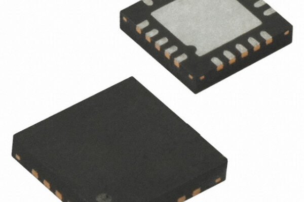
•High-Frequency Traces: LPWAN modules (e.g., LoRa, NB-IoT) operate at sub-1 GHz frequencies (e.g., 868 MHz, 915 MHz). Ensure controlled impedance (50Ω single-ended/85Ω differential) and use low-loss substrates (e.g., FR4 with Df < 0.02) to minimize attenuation.

•Antenna Integration: Antennas must be isolated from noise sources (e.g., power supplies). For compact designs, use ceramic or PCB-embedded antennas.
•Shielding: Employ grounded copper pours and shielded cans to suppress EMI, especially in dense mixed-signal layouts.
4.2 Power Management
•Low-Power Design: Implement efficient power regulation (e.g., LDOs for noise-sensitive circuits, buck converters for high efficiency). Use decoupling capacitors (100 nF–10 μF) near LPWAN ICs to stabilize voltage.
•Battery Optimization: For battery-operated devices, leverage power-saving modes (e.g., PSM, eDRX) to extend lifespan. Ensure sleep currents remain <1 μA.
4.3 Thermal Management
•Heat Dissipation: LPWAN power amplifiers (PAs) can generate heat during transmission. Use thermal vias and copper pours under ICs to dissipate heat.
•Component Placement: Avoid locating heat-sensitive components (e.g., sensors) near PAs or voltage regulators.
4.4 Mechanical and Environmental Robustness
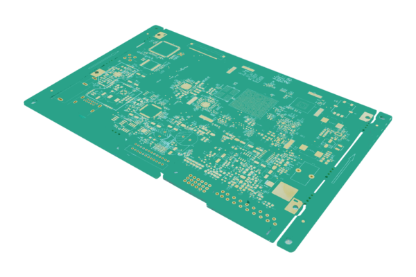
•Compact Layouts: LPWAN devices often deploy in tight spaces (e.g., sensors in industrial equipment). Use HDI techniques (e.g., microvias, 0.4 mm trace/space) for miniaturization.
•Conformal Coating: Protect boards from moisture, dust, and chemicals in harsh environments (e.g., agriculture, logistics).
5. Advanced PCB Strategies for LPWAN Systems
•Hybrid Architectures: Combine LPWAN with short-range protocols (e.g., BLE, Zigbee) for multi-connectivity.
•Modular Designs: Use pre-certified LPWAN modules (e.g., Murata’s LoRaWAN modules) to reduce time-to-market and simplify RF design.
•Additive Manufacturing: For low-volume, high-customization projects, 3D-printed PCBs enable rapid prototyping of unique form factors.
6. Future Trends and Opportunities
•5G Integration: LPWAN will complement 5G for massive IoT, with NB-IoT evolving as a 5G technology.
•AI and Edge Computing: On-device AI for data preprocessing will reduce transmission overhead.
•Standardization: Efforts by FiRa Alliance and 3GPP will enhance interoperability.
•Sustainability: LPWAN’s low energy footprint aligns with green IoT initiatives.
7. How PCB Enterprises Can Adapt
•Invest in RF Expertise: Train designers on high-frequency layout tools (e.g., ANSYS HFSS) and antenna tuning.
•Collaborate with Chipset Providers: Partner with Semtech (LoRa), Huawei (NB-IoT), and emerging players (e.g., TurMass) for early access to SDKs and reference designs.
•Focus on Testing: Validate designs for compliance with LPWAN protocols (e.g., LoRaWAN Class A/B/C) and regulatory standards (FCC, CE).
Conclusion
LPWAN technology is reshaping IoT connectivity, offering unparalleled range, power efficiency, and scalability. For PCB enterprises, success hinges on mastering high-frequency design, power management, and miniaturization techniques. By embracing modular approaches, advanced materials, and industry collaborations, your business can lead the charge in smart cities, industrial IoT, and beyond—enabling a seamlessly connected world.
Get your exclusive quote immediately: fill out the form or send an email directly.As a professional PCB manufacturer for hobbyist , we will provide you with a quote service within 24 hours. Enjoy free DFM optimization and a 10% discount on SMT patches for your first order!