Introduction: From “Bandwidth Bottleneck” to “OSFP Deployment” — An Inevitable Choice in the High-Speed Interconnect Era
The exponential growth of data-intensive applications—such as AI, cloud computing, and 5G—has pushed traditional connectivity solutions to their limits. Bandwidth bottlenecks in data centers and telecommunications infrastructure demand faster, more efficient interconnect technologies. Enter the Octal Small Form-factor Pluggable (OSFP) connector system, a groundbreaking solution designed to support 400G/800G data rates and beyond. For PCB enterprises, OSFP represents both a challenge and an opportunity: It requires advanced design and manufacturing capabilities but unlocks new markets in high-performance computing, AI clusters, and next-generation data centers. This article explores OSFP’s technical foundations, market drivers, PCB-specific challenges, and strategic pathways for industry adoption.
Table of Contents
1. OSFP Basics: Definition, Advantages, and Industry Standards
OSFP is a high-density, pluggable connector system developed to address the need for higher bandwidth and better thermal management in data centers. Key features include:
– High Data Rates: Supports 56 Gbps to 112 Gbps PAM-4 per channel, enabling aggregate speeds of 400G/800G (with 1.6T in development).
– Thermal Efficiency: Its slightly larger form factor (compared to QSFP-DD) improves airflow and heat dissipation, critical for high-power applications (e.g., 25W modules).
– Compliance and Compatibility: Adheres to OSFP MSA (Multi-Source Agreement) and IEEE 802.3ck standards, ensuring interoperability with existing infrastructure (e.g., backward compatibility with 56 Gbps interfaces).
– Signal Integrity: Strict tolerance controls for terminal width/spacing and robust grounding mechanisms minimize crosstalk and EMI.
Industry Standards: OSFP is backed by major players like Google, Arista Networks, and TE Connectivity, with specifications covering electrical interfaces, thermal management, and mechanical designs.

2. Market Drivers and Applications: Where PCB Demand Lies
The demand for OSFP is fueled by:
– AI and HPC Workloads: AI training clusters (e.g., NVIDIA’s GPU systems) require low-latency, high-throughput interconnects. OSFP-based 800G/1.6T optical modules are becoming the norm.
– Data Center Expansion: Hyperscale data centers need higher port density (e.g., 36 ports per 1RU switch) and energy-efficient solutions.
– Telecommunications: 5G infrastructure and edge computing rely on OSFP for fronthaul/backhaul networks.
– Consumer Electronics: Emerging applications in AR/VR and autonomous vehicles will eventually adopt OSFP-derived technologies.
PCB-Specific Opportunities:
– Motherboards and Switch PCBs: High-layer count (12+ layers) designs with controlled impedance traces.
– Thermal Management Solutions: PCBs with embedded heat sinks, thermal vias, and low-CTE materials.
– Optical Modules: PCBs for OSFP-based transceivers require low-loss dielectrics (e.g., Rogers substrates) and precise impedance matching.
3. Technical Challenges for PCBs: From Performance to Reliability
Integrating OSFP into PCBs introduces multifaceted challenges:
Signal Integrity
– High-Frequency Loss: OSFP’s 112 Gbps PAM-4 signals operate at Nyquist frequencies up to 32 GHz, necessitating low-loss materials (Df < 0.005) and 85Ω differential pairs.
– EMI Control: Shielding techniques (e.g., grounded copper pours) and isolation zones are critical to prevent interference.
Thermal Management
•Heat Dissipation: High-power OSFP modules (e.g., 25W) require thermal vias, copper cores, and advanced cooling solutions (e.g., graphene heat sinks).
•CTE Matching: Low-CTE glass fiber substrates (e.g., Asahi 1017) prevent warping under thermal stress.
Mechanical Reliability
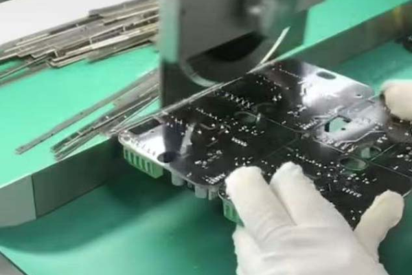
•Connector Integration: OSFP’s 60-pin interface (0.6 mm pitch) demands precise solder joint control and belly-to-belly mounting for low-noise performance.
•Durability: PCBs must withstand repeated plugging/unplugging cycles and mechanical stress.
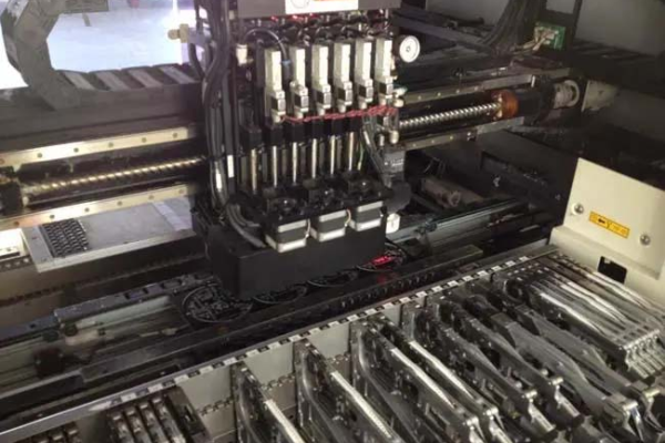
Manufacturing Complexity
•Tolerances: Tight controls for impedance (±10%) and layer alignment are essential.
•Testing: High-frequency testing (e.g., TDR, VNA) and protocol validation (e.g., PAM-4 eye diagrams) are mandatory.
4. Strategic Responses for PCB Enterprises: Technology Investment and Capability Upgrades
To capitalize on OSFP opportunities, PCB manufacturers must:
– Adopt Advanced Materials: Invest in low-loss dielectrics (e.g., Rogers, Megtron 6) and low-CTE glass fibers for improved signal and thermal performance.
– Enhance Design Capabilities: Leverage HFSS/CST simulations for signal integrity analysis and thermal modeling tools for heat management.
– Optimize Processes: Implement laser drilling for microvias, controlled impedance routing, and automated optical inspection (AOI) for quality assurance.
– Collaborate with Ecosystem Partners: Work with OSFP connector suppliers (e.g., Molex, TE Connectivity) and chipset providers (e.g., Broadcom, Credo) for early access to reference designs.
– Focus on Testing and Validation: Develop in-house labs for TDR testing, EMI/EMC validation, and protocol compliance (e.g., IEEE 802.3ck).

5. Future Outlook: OSFP Evolution and the PCB Industry’s New Role
OSFP technology is rapidly evolving:
– 1.6T OSFP Modules: Already in development (e.g., light-sensitive technology’s 3nm DSP-based solutions), requiring PCBs with even higher signal integrity and thermal resilience.
– Co-Packaged Optics (CPO): OSFP will play a role in CPO architectures, where PCBs integrate optical engines alongside ASICs.
– Sustainability: OSFP’s energy-efficient design aligns with green data center initiatives, reducing CO2 emissions.
For PCB Enterprises, this means:
– Transitioning from mere board suppliers to solution providers offering integrated thermal, signal, and power management.
– Expanding into optical PCB substrates and embedded component technologies.
6. Collaboration Invitation: Building the OSFP High-Speed Interconnect Ecosystem
The complexity of OSFP requires cross-industry collaboration. We invite:
– Connector Manufacturers: To jointly develop PCB-compatible OSFP solutions (e.g., optimized landing patterns).
– Chipset Developers: To share reference designs and signal integrity models.
– Data Center Operators: To provide real-world requirements for reliability and performance.
– Research Institutions: To advance materials science (e.g., nano-coated substrates for lower loss).
Our Commitment: As a PCB enterprise, we are investing in OSFP-ready production lines, R&D partnerships, and industry-standard compliance to drive this ecosystem forward.
Conclusion
OSFP technology is not just an incremental upgrade but a transformative leap in high-speed interconnectivity. For PCB enterprises, mastering its challenges—signal integrity, thermal management, and mechanical reliability—is key to unlocking opportunities in AI, data centers, and beyond. By embracing advanced materials, design innovations, and collaborative ecosystems, your business can lead the charge into the terabit-era of connectivity.
Get your exclusive quote immediately: fill out the form or send an email directly.As a professional PCB manufacturer for hobbyist , we will provide you with a quote service within 24 hours. Enjoy free DFM optimization and a 10% discount on SMT patches for your first order!