Introduction
Underfill technology is a critical process in modern electronics manufacturing, particularly for PCB enterprises aiming to enhance the reliability and durability of advanced packaging solutions such as FC (Flip-Chip), BGA (Ball Grid Array), and CSP (Chip Scale Package). This polymer-based filling technique addresses thermal expansion coefficient (CTE) mismatches between chips and substrates, significantly improving resistance to thermal stress, mechanical shock, and environmental factors. For PCB manufacturers, mastering underfill processes is essential to meet the demands of high-performance applications in automotive, AI, consumer electronics, and beyond. This article explores the principles, types, applications, and PCB-specific considerations of underfill technology, providing insights into how your business can leverage this technique to drive innovation and quality.
Table of Contents
1. What Is Underfill Technology?
Underfill involves injecting a polymer-based material (typically epoxy resin filled with SiO2) into the gap between a semiconductor chip and its substrate. After curing, this material forms a robust layer that:
– Reduces Thermal Stress: Mitigates CTE mismatches (e.g., silicon chip CTE: 2.8 ppm/°C vs. FR-4 PCB CTE: 15.8 ppm/°C) .
– Enhances Mechanical Strength: Improves resistance to vibration, shock, and drop impacts (e.g., 10–100x increase in solder joint fatigue life) .
– Protects Environmental Damage: Shields solder joints from moisture, dust, and corrosion .
Originally developed by IBM in the 1970s, underfill has evolved to support miniaturized, high-density PCB designs .

2. Types of Underfill Processes
Four mainstream underfill techniques are used in PCB manufacturing, each with unique advantages and challenges :
2.1 Capillary Underfill (CUF)
•Process: Epoxy is dispensed along the chip edge, capillary action draws it into the gap, followed by thermal curing (120–165°C for minutes to hours) .
•Applications: FC, BGA, CSP packages.
•Advantages: High reliability, compatibility with diverse packages.
•Challenges: Slow process, risk of voids, inefficient for large chips .
2.2 No-Flow Underfill (NUF)
•Process: Epoxy is pre-dispensed before chip placement; reflow soldering simultaneously forms solder joints and cures the underfill .
•Applications: CSP, BGA, and POP (Package-on-Package).
•Advantages: Simplified workflow, reduced process time.
•Challenges: Potential bubbles/voids, limited filler content, higher CTE .
2.3 Wafer-Level Underfill (WLUF)
•Process: Underfill is applied and partially cured at the wafer level before dicing; chips are then attached via standard SMT .
•Applications: Flip-chip packages.
•Advantages: High throughput, SMT compatibility.
•Challenges: Low filler content may reduce thermal stability .
2.4 Molded Underfill (MUF)
•Process: Combines underfill and overmolding in a single step using transfer molding equipment .
•Applications: Multi-chip modules, FC-CSP, FC-BGA.
•Advantages: 4x faster productivity, excellent for miniaturization (fills gaps as small as 40 μm).
•Challenges: Difficult rework, requires specialized molds .
3. Why Underfill Matters for PCB Enterprises
3.1 Reliability in Harsh Environments
•Underfill is indispensable for automotive and industrial PCBs exposed to temperature cycles (-40°C to 150°C) and mechanical vibration. For example, Meig Smart’s automotive modules use underfill to achieve AEC-Q104 compliance .
3.2 Support for Advanced Packaging
•As PCBs integrate more BGA/CSP components (e.g., 20+ BGA chips per module in automotive SIPs), underfill prevents solder joint failure due to CTE mismatch .
3.3 Miniaturization Demands
•Underfill enables finer pitch designs (e.g., ≤0.3 mm CSP pitch) and 3D stacking (POP), critical for smartphones, wearables, and AI hardware .
4. PCB Design Considerations for Underfill
Successful underfill implementation requires careful PCB design :
– Component Spacing: Maintain ≥0.7 mm clearance from other components for dispense needle access .
– Pad Design: Smaller pads with wider spacing improve filler flow and reduce voids .
– Surface Finish: Eliminate exposed copper and ensure solder mask covers all non-pad areas to prevent wetting issues .
– Flatness: PCBs must be flat to avoid uneven filler distribution; avoid trenches or grooves in solder mask .
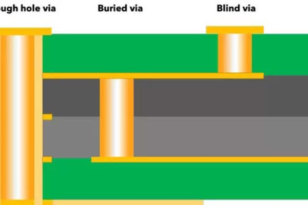
– Via Handling: Fill microvias and cover with solder mask to prevent air entrapment .

5. Process Challenges and Solutions
•Voids/Bubbles: Caused by flux residues or rapid curing. Solution: Pre-clean PCBs with eco-friendly systems (e.g., MK-AIseries selective cleaning) and use vacuum curing .
•Slow Flow: High-viscosity epoxies delay filling. Solution: Pre-heat PCBs to 60–90°C to reduce viscosity .
•Rework Difficulty: Traditional underfills are hard to remove. Solution: Use reworkable epoxies (e.g., Loctec 3515/3568) .
6. Industry Applications and Case Studies
•Automotive: Meig Smart’s underfill+BGA process enhances module mechanical strength and thermal performance for SA8155P-based telematics units .
•Consumer Electronics: Smartphones use underfill to survive 2-meter drops by absorbing impact energy .
•High-Frequency PCBs: Low-Dk/Df underfills (e.g., WLUF) minimize signal loss in 5G/mmWave designs .
7. Future Trends
•Material Innovations: Nano-filled epoxies with lower CTE (<10 ppm/°C) and higher thermal conductivity (>1 W/mK) .
•Advanced Equipment: Precision jetting systems (e.g., Tensun’s Sherpa900) enable tilt dispensing for better fillet control .
•Integration with SIP: Underfill becomes vital for system-in-package modules combining multiple ICs .
8. How PCB Enterprises Can Adapt
•Invest in Automation: Deploy automated dispensing and curing systems to ensure consistency.
•Collaborate with Material Suppliers: Partner with epoxy vendors (e.g., Henkel, Hanse) for customized solutions.
•Prioritize Testing: Implement shear testing, thermal cycling (-55°C to 125°C), and acoustic microscopy to detect voids.
Conclusion
Underfill technology is no longer optional but a necessity for PCB enterprises targeting high-reliability markets. By adopting advanced underfill processes—whether CUF, NUF, WLUF, or MUF—your business can overcome CTE challenges, enhance product longevity, and capture opportunities in automotive, AI, and IoT. Embrace material innovations, precision equipment, and robust design practices to lead the next wave of electronic manufacturing.
Get your exclusive quote immediately: fill out the form or send an email directly.As a professional PCB manufacturer for hobbyist , we will provide you with a quote service within 24 hours. Enjoy free DFM optimization and a 10% discount on SMT patches for your first order!