Diodes are fundamental components in electronics that allow current to flow in only one direction, acting as a one-way valve for electrical current. They are widely used in various applications, from rectification to voltage regulation and signal modulation. Understanding their typical characteristics and how they are applied in circuits is essential for designing reliable electronic systems.
This article Shenzhen PCBA manufacturer SysPCB will discuss the role and working principle of special-purpose diodes. Then, this article will take Skyworks Solutions and ON Semiconductor’s products as examples to discuss the typical characteristics of these diodes, and finally will provide some circuit examples to show how to use them effectively.
Table of Contents
Typical Diode Characteristics
Before diving into circuit examples, it’s important to first understand the typical characteristics of diodes, which include their voltage-current relationship, forward voltage, reverse bias behavior, and other parameters.
a. Forward Voltage Drop (V_f)
When a diode is forward biased (i.e., the positive terminal of the power supply is connected to the anode and the negative terminal to the cathode), it starts to conduct once the voltage exceeds a certain threshold, known as the forward voltage drop. This value varies depending on the type of diode:
Silicon Diodes: Typically have a forward voltage drop of about 0.7V. This means that the diode will not conduct significantly until the voltage at the anode exceeds 0.7V.
Germanium Diodes: Have a lower forward voltage drop, typically around 0.3V.
Schottky Diodes: These are made of metal-semiconductor junctions and have a much lower forward voltage drop, usually between 0.2V and 0.45V.
b. Reverse Breakdown Voltage (V_R)
When a diode is reverse biased (i.e., the positive terminal of the power supply is connected to the cathode and the negative terminal to the anode), ideally, it should not conduct any current. However, if the reverse voltage exceeds a certain threshold, called the reverse breakdown voltage, the diode will start to conduct in the reverse direction. For regular diodes, this is typically very high (in the range of tens or hundreds of volts), but in Zener diodes, the reverse breakdown is utilized deliberately for voltage regulation.
c. Reverse Leakage Current (I_R)
In reverse bias, a small current may still flow through the diode even before it reaches breakdown, due to reverse leakage current. This current is usually very small (in the nanoampere range for most diodes) and can be significant only when the reverse voltage approaches the breakdown region.
d. Capacitance
Diodes exhibit a junction capacitance between the anode and cathode, especially when they are reverse biased. This capacitance can be a critical factor in high-frequency applications, such as in radio-frequency (RF) circuits, where the diode’s switching characteristics play a significant role.
e. Speed of Switching
The reverse recovery time (t_rr) is a characteristic that defines how quickly a diode can switch from conducting to non-conducting states. Fast switching diodes, such as Schottky diodes, have very low reverse recovery times, making them ideal for high-speed circuits.
Common Diode Types and Their Applications
Several types of diodes are used for different applications, each with specific characteristics that make them suitable for particular tasks:
Standard Diodes: Used for general-purpose rectification in power supplies.
Zener Diodes: Designed for voltage regulation. Zener diodes allow current to flow in the reverse direction when the voltage exceeds a certain value (the Zener voltage), maintaining a stable voltage.
Schottky Diodes: Known for their low forward voltage drop and fast switching speed. These are often used in power rectifiers and high-speed circuits.
Light Emitting Diodes (LEDs): These emit light when forward biased and are used in display technologies, lighting, and indicators.
Photodiodes: These are used in optical applications where the diode generates current in response to light exposure.
Diodes for Protection (TVS Diodes, Varistors): Used to protect sensitive circuits from voltage spikes or transients.
Varactor diode
Varactor diodes are junction diodes suitable for providing variable capacitance. The P-N junction is reverse biased, and the diode capacitance can be changed by changing the applied DC bias (Figure 1).
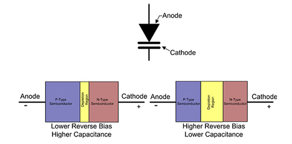
Figure 1: Varactor diodes provide variable capacitance based on the applied reverse bias. The higher the bias voltage level, the lower the capacitance. (Source: Digi-Key Electronics)
The capacitance of the varactor diode is inversely proportional to the applied DC bias. The higher the reverse bias voltage, the wider the depletion region of the diode, and therefore the lower the capacitance. In Skyworks Solutions’SMV1801-079LF hyperabrupt junction varactor diode capacitance and reverse bias curve, we can see this change graphically (Figure 2).
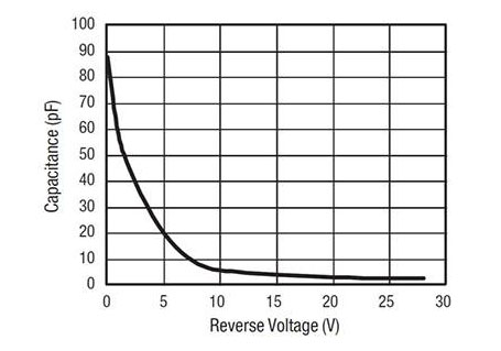
Figure 2: The capacitance of the SMV1801-079LF varactor diode of Skyworks Solutions as a function relation of reverse bias. (Source: Skyworks Solutions)
These diodes have a very high breakdown voltage and a bias of up to 28 volts, which can be applied in a wide tuning range. The control voltage must be applied to the varactor diode to avoid flipping the next stage of the bias; it usually uses capacitive coupling, as shown in Figure 3.
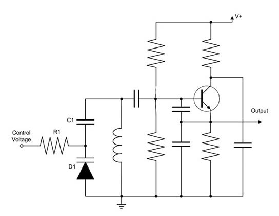
Figure 3: The varactor diode tuned oscillator alternating current coupling the varactor diode D1 to the oscillator through capacitor C1. This isolates the varactor diode D1 from the transistor bias and vice versa. The control voltage is applied through resistor R1. (Source: Digi-Key Electronics)
Varactor diodes can replace variable capacitors in other applications, such as tuned RF or microwave filters, frequency or phase modulators, phase shifters, and frequency multipliers.
PIN diode
PIN diodes are used as switches or attenuators at RF and microwave frequencies. It is formed by stacking a high-resistivity intrinsic semiconductor layer between the P-type layer and the N-type layer of a conventional diode.
Unbiased or reverse biased diodes have no charge stored in the intrinsic layer. This is the turn-off condition for switching applications. Inserting an intrinsic layer can increase the effective width of the diode depletion layer, resulting in very low capacitance and increased breakdown voltage.
The forward bias condition causes holes and electrons to be injected into the intrinsic layer. These carriers take some time to recombine with each other. This time is called the carrier lifetime “t”. The average stored charge reduces the effective resistance of the intrinsic layer to the minimum resistance “RS”. Under forward bias conditions, the diode acts as an RF attenuator.
Skyworks SoluTIons’ SMP1307-027LF PIN diode array combines four PIN diodes in a common package and serves as an RF/microwave attenuator in the frequency range of 5 MHz to 2 GHz (Figure 4).
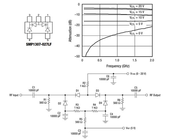
Figure 4: PIN diode attenuator circuit based on Skyworks Solutions’ SMP1307-027LF PIN diode array. The graph uses the control voltage as a parameter to show the relationship between attenuation and frequency. (Source: Skyworks Solutions)
The PIN diode array is suitable for low-distortion Pi and T-shaped configuration attenuators. Based on the 1.5 microsecond (µs) carrier lifetime, the effective resistance RS does not exceed 100 Ω at 1 mA and 10 Ω at 10 mA. It is suitable for TV signal distribution applications.
Schottky diode
Schottky diodes, are manufactured based on metal-semiconductor junctions (Figure 5). The metal side of the junction forms the anode, and the semiconductor side becomes the cathode. When forward biased, Schottky diodes have a maximum forward voltage drop in the range of 0.2 to 0.5 volts, depending on the forward current and diode type. When a Schottky diode is used in series with a power supply, such as in a reverse voltage protection circuit, such a low forward voltage drop is very useful because it can reduce power loss.
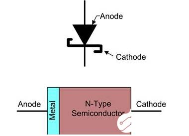
Figure 5: The physical structure of a Schottky diode is based on a metal-N-type semiconductor junction, and therefore has a very low forward voltage drop and extremely fast switching speed. (Source: Digi-Key Electronics)
Another important characteristic of these diodes is the very fast switching speed. When switching from the on state to the off state, a standard diode takes a certain amount of time to eliminate the charge in the depletion layer. Unlike a Schottky diode, the metal-semiconductor junction has no associated depletion layer.
Compared with silicon junction diodes, Schottky diodes have limited peak reverse voltage ratings. Therefore, they are usually limited to low-voltage switch mode power supplies. ON Semiconductor’s 1N5822RLG peak reverse voltage (PRV) is rated up to 40 volts and has a maximum forward current of 3 A. It can be applied in many aspects of switch mode power supplies (Figure 6).
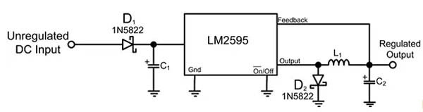
Figure 6: Typical application examples of Schottky diodes in switch mode power supplies, including for reverse power protection (D1) and transient suppression (D2). (Source: Digi-Key Electronics)
Schottky diodes can be used to protect the regulator circuit from accidental application of reverse polarity at the input. The diode D1 in this example is used for this purpose. The main advantage of this diode in this application is the low forward voltage drop. Another more important function of the Schottky diode (D2 in this example) is to provide a return path when the switch is closed, allowing current to flow through the inductor L1. D2 must be a fast diode connected with a short low-inductance to achieve this function. In this application of low-voltage power supply, Schottky diode has excellent performance.
Schottky diodes can also be used in RF designs. Their fast switching, low forward voltage drop, and low capacitance make them ideal for detectors and sample-and-hold switches.
Zener diode
The Zener diode can maintain a fixed voltage when it is reverse biased. This function can be used to provide a known reference voltage, this is an important operation in power supplies. Zener diodes can also be used to clip or limit the waveform to prevent them from exceeding the voltage limit.
Zener diodes are manufactured using heavily doped P-N junctions, so the depletion layer is very thin. This area generates a very high electric field, even when a lower voltage is applied. Under these conditions, the following two mechanisms cause the diode to break down, resulting in a high reverse current:
1. Zener breakdown occurs at a voltage less than 5 volts, which is the result of electron quantum tunneling.
2. Breakdown mechanism is the breakdown due to avalanche breakdown or impact ionization when the voltage is higher than 5 volts.
In both cases, the operation of the diode is similar (Figure 7).

Figure 7: Schematic symbol of Zener diode and its current-voltage characteristic curve. Although the current-voltage characteristic of the Zener diode has a normal forward conduction region, but when reverse bias occurs, it will break down and maintain a constant voltage across the diode. (Source: Digi-Key Electronics)
When the Zener diode is forward biased, it can be used as a standard diode. When receiving a reverse bias, if the reverse bias level exceeds the Zener voltage level VZ, it will break down. At this time, the diode maintains a nearly constant voltage between the cathode and anode. The minimum current to keep the diode in the Zener breakdown region is IZmin; the maximum current determined by the rated power dissipation of the diode is IZmax. The current must be limited by external resistors to prevent overheating and malfunctions. This is shown in the schematic diagram of the basic voltage regulator based on the Zener effect in Figure 8, which is constructed using ON Semiconductor’s 1N5229B Zener diode.
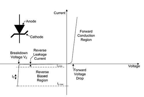
Figure 8: Schematic diagram of a basic voltage regulator using a Zener diode, and load regulation response. (Source: Digi-Key Electronics)
The maximum power consumption of the 1N5229B Zener diode is 500 milliwatts (mW), and the nominal Zener voltage is 4.3 volts. With no load, a 75 ohm (Ω) series resistor (R1) limits power dissipation to 455 mW. As the load current increases, the power dissipation will decrease. The figure shows the load regulation curve when the load resistance value is 200 ohm to 2,000 ohm.
In addition to voltage regulation, Zener diodes can also be wired back-to-back to provide a controlled voltage limited to the Zener voltage, as well as a forward voltage drop value. The 4.3 volt Zener limiter will be limited to ±5 volts. Limiting applications can be extended to a wider range of overvoltage protection circuits.
Conclusion
Diodes are versatile components with a wide range of applications in electronic circuits. By understanding their characteristics—such as forward voltage drop, reverse breakdown voltage, and switching speed—engineers can design circuits that leverage the unique properties of different diode types. Whether used for rectification, voltage regulation, signal clipping, or light emission, diodes are essential building blocks in modern electronic design.