In low-power electronic systems such as real-time clocks (RTC), smartwatches, and IoT devices, the 32.768kHz crystal oscillator is responsible for the core function of precise timing. However, industry data shows that over 70% of crystal oscillator failures are caused by load capacitor mismatch or PCB design defects, which can result in time errors or equipment functional paralysis. This article will delve into the mechanism of vibration stoppage and provide a comprehensive solution from diagnosis to prevention.
Table of Contents
1、 Deep analysis of the reasons for non oscillation
1. Electrical characteristic mismatch (accounting for 55%)
-Load capacitance deviation
The crystal oscillator frequency is determined by the load capacitance (C<sub>L</sub>), and the calculation formula is:
C_L = (C1 × C2)/(C1 + C2) + C_stray
Among them, C1/C2 is the external matching capacitor, and Cstray is the parasitic capacitance of PCB routing (about 0.5pF/10mm). Common errors include:
-Misuse of 22pF capacitor leads to excessive C<sub>L</sub>and frequency deviation>100ppm
-Neglecting the routing capacitance results in actual C<sub>L</sub>deviating from the nominal value (usually 6-12pF)
-Insufficient negative resistance
Vibration margin requirement: | Negative resistance |>5 × R<sub>ESR</sub>(R<sub>ESR</sub>usually 30-100k Ω). Failure scenarios include:
-Insufficient internal driver gain of MCU (such as STM32L0 requiring external amplification circuit)
-The power supply voltage is lower than the startup threshold (1.8V system mistakenly selects 3.3V crystal oscillator)
2. Physical damage and environmental interference (accounting for 30%)
-Welding thermal stress
Reflow peak temperature>260 ℃ or>220 ℃ for>60 seconds, causing microcracks in the chip. Surface mount crystal oscillators (such as 3215 package) are particularly sensitive
-Mechanical stress failure
When the bending of the plate is greater than 0.5%, the internal electrodes of the crystal oscillator break, which is common in devices near the edge of the plate or screw holes
-EMI interference
High frequency noise is coupled through power lines (Δ V>50mV) or parallel wiring (>10mm), resulting in frequency offset
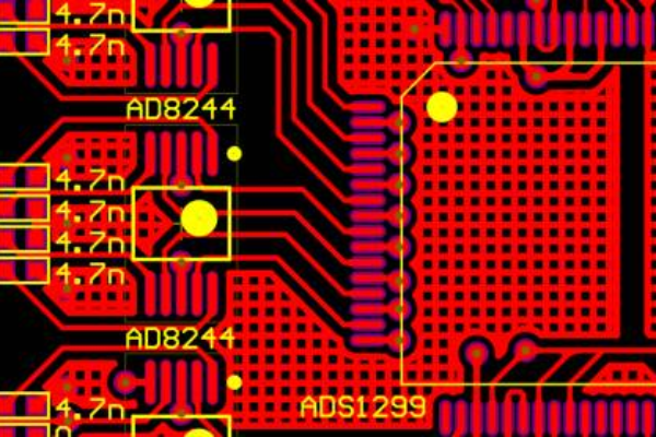
3. PCB design defects (accounting for 15%)
| Error type | Consequences | Design specifications |
| Wire length>30mm | Signal phase shift>20 ° | ≤ 10mm |
| Reference layer cross segmentation | Impedance mutation causing reflection | Complete GND plane |
| Wiring between crystal oscillator pins | Frequency offset caused by capacitive coupling | No crossing of wires allowed |
| Match capacitor away from crystal oscillator | Introduce additional parasitic inductance | Distance from pin ≤ 2mm |
2、 Systematic solution
1. Electrical parameter calibration
-Accurate matching of load capacitance
Select C1/C2 according to the formula:
C1=C2=2 × (C_L – C_stray)//C_stray is estimated at 2-3pF
Use capacitors made of NP0/C0G material with a tolerance of within ± 5%
-Negative resistance testing and compensation
1. Series connected 1M Ω variable resistor R<sub>test</sub>
2. Increase R<sub>test</sub>until the vibration stops, the critical value is | negative resistance|
3. If | negative resistance |<5 × R<sub>ESR</sub>, replace the low ESR crystal oscillator or add an amplifier
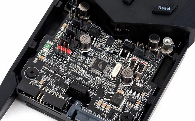
2. PCB design optimization
-Layout Iron Law

-The distance between the crystal oscillator and MCU is ≤ 15mm. The wiring is wrapped around the ground and shielded through holes are added (spacing ≤ 15mm)
-Single point grounding: The GND pin of the crystal oscillator is directly connected to the GND pin of the MCU, and it is prohibited to connect it through copper plating
-Power filter
Parallel connection of 10nF ceramic capacitor and 1 μ F tantalum capacitor at the power supply end to suppress voltage fluctuations
3. Process and environmental control
-Optimization of Welding Curve
-Heating slope ≤ 2 ℃/s
-Duration above 220 ℃ ≤ 40 seconds
-Peak temperature ≤ 260 ℃ (recommended high-temperature resistant crystal oscillator such as EPSON MC-306)
-Anti interference reinforcement
-Copper grounding around the crystal oscillator (spacing ≥ 0.3mm)
-Temperature compensated crystal oscillator (TCXO) is selected for extreme environments
4. Ultimate solution: Active crystal oscillator replacement
When the passive crystal oscillator repeatedly fails, switching to an active crystal oscillator (OSC) can completely solve the problem:
| Characteristics | Passive crystal oscillator | Active crystal oscillator |
| Vibration reliability | requires external matching | built-in oscillation circuit |
| Anti-interference ability | weak | strong (-40dB suppression) |
| Cost | Low ($0.1~0.3) | High ($0.5~1.2) |
| Applicable scenarios | Consumer electronics | Industrial/medical equipment |
>Case: A medical monitor RTC stopped vibrating due to C1/C2=15pF (nominal C<sub>L</sub>=7pF). After replacing with a 6.8pF capacitor and reducing the wiring from 25mm to 8mm, the frequency deviation is less than 5ppm and the 72 hour time error is less than 1 second.
3、 Preventive design strategy
1. Prevention during the design phase
-Simulation first
Simulate oscillation margin using SPICE model to ensure | negative resistance |>5 × R<sub>ESR</sub>
-Fault tolerant design
Reserved capacitor pads (such as 6.8pF/8.2pF/10pF) for easy parameter adjustment
2. Material selection specifications
-Priority car grade crystal oscillator
Select AEC-Q200 certified devices (such as EPSON MC-146) with a working temperature of -40~105 ℃
-Verify key parameters
-Frequency deviation ≤± 20ppm
-Aging rate<± 3ppm/year
3. Production and testing control
-Process monitoring
Real time recording of reflow soldering furnace temperature curve, isolation re inspection of boards above 220 ℃ for more than 40 seconds
-Automated testing
Using a flying needle tester to measure:
-Start time (<2 seconds is qualified)
-Output voltage V<sub>pp</sub>>0.3V (1.8V system)
Summary: Building a three-level defense system
1. Design defense: Following the 3W wiring rule (line spacing ≥ 3 x line width), the GND isolation ring surrounds the crystal oscillator
2. Material defense: Select ± 10ppm industrial grade crystal oscillator and match load with NP0 capacitor
3. Process defense: Welding curve compliance testing, 100% negative resistance testing
>[Download the “32.768kHz Crystal Oscillator Design Checklist”]
Including capacitance calculation tools, PCB routing specifications, and production line testing protocols
Through the triple guarantee of electrical calibration, design reinforcement, and process control, 99% of vibration stoppage faults can be completely solved. When reliability requirements are stringent, active crystal oscillators are still the ultimate choice – their additional costs are much lower than the losses from fault recalls.
Get your exclusive quote immediately: fill out the form or send an email directly, and we will provide you with a quote service within 24 hours. Enjoy free DFM optimization and a 10% discount on SMT patches for your first order!