The silkscreen layer in a printed circuit board (PCB) plays a crucial role in identifying components, providing assembly instructions, and ensuring ease of maintenance. This article provides an overview of the PCB silkscreen layer, its applications, design considerations, and best practices to enhance PCB manufacturing and usability.
Table of Contents
1. What is the PCB Silkscreen Layer?
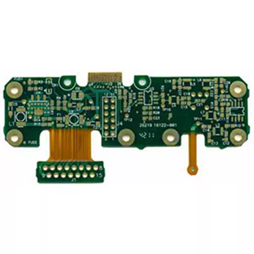
The PCB silkscreen layer is a non-conductive ink layer applied to the surface of a PCB to provide printed markings. These markings include component designators, polarity indicators, logos, warning symbols, and other essential information.
Common Elements in a Silkscreen Layer:
Component Labels: Designators (e.g., R1, C2, U3) that help in identifying components.
Polarity and Orientation Markings: Indications for diodes, LEDs, and polarized capacitors.
Test Points and Reference Designators: Labels for testing and debugging purposes.
Company Logos and Manufacturing Information: Brand identifiers and production details.
Warnings and Safety Labels: Indications for high voltage and special handling requirements.
2. Silkscreen Printing Techniques
Several methods are used to apply the silkscreen layer to a PCB, each with its own advantages and limitations.
Common Silkscreen Printing Methods:
Manual Screen Printing: Uses a stencil and ink to print markings. Suitable for low-volume production.
Liquid Photo Imaging (LPI): Provides higher precision and is suitable for fine details and dense PCBs.
Direct Legend Printing (DLP): Uses inkjet printing technology for high-resolution and cost-effective labeling, ideal for complex and high-density boards.
3. Design Considerations for PCB Silkscreen
To ensure readability and manufacturability, designers must follow certain guidelines when creating the silkscreen layer.
Best Practices for Silkscreen Design:
Font Size and Line Thickness: Maintain a minimum font size of 0.8 mm and a line width of at least 0.15 mm to ensure readability.
Contrast and Placement: Use white or yellow silkscreen ink on dark solder masks for visibility.
Avoid Overlapping Pads: Ensure silkscreen text does not cover solder pads or vias to prevent manufacturing issues.
Layer Selection: Apply silkscreen to the top and/or bottom layers, avoiding areas covered by solder masks.
Component Alignment: Ensure text is oriented consistently to improve readability and assembly efficiency.
4. Importance of the Silkscreen Layer
The silkscreen layer offers several benefits to PCB assembly, troubleshooting, and repair.
Key Advantages:
Enhances Assembly Efficiency: Clear labeling helps assembly technicians quickly identify components.
Improves Debugging and Maintenance: Engineers can easily locate test points and components during troubleshooting.
Increases Manufacturing Precision: Well-placed silkscreen markings help avoid errors in PCB production.
Supports Regulatory Compliance: Safety markings ensure adherence to industry standards.
Conclusion
The PCB silkscreen layer is an essential aspect of circuit board design, providing valuable information for assembly, testing, and maintenance. By following proper design practices and using appropriate printing techniques, designers can ensure clear and effective silkscreen markings that enhance the functionality and usability of the PCB.