Printed Circuit Boards (PCBs) rely on different types of holes for electrical and mechanical connectivity. Two critical types of holes in PCB design and manufacturing are through-holes and via holes. These holes play a fundamental role in establishing electrical connections between different PCB layers and ensuring structural integrity. This article explores the differences, applications, and technological advancements in through-hole and via hole technology in PCBs.
Table of Contents
Through-Hole Technology (THT)
1. What is the definition and function of through-hole technology?
Through-hole technology (THT) involves inserting electronic components with leads into pre-drilled holes on a PCB and soldering them to pads on the opposite side. This technique creates strong mechanical and electrical connections, making it suitable for applications requiring durability and high reliability.
2. What are Types of Through Horace?
Plated Through-Holes (PTH): These holes have conductive plating along their inner walls, allowing electrical signals to pass between PCB layers.
Non-Plated Through-Holes (NPTH): These holes lack conductive plating and are used primarily for mechanical mounting rather than electrical connectivity.
3. What are the advantages of THT?
Strong Mechanical Bonds: Ideal for components subject to mechanical stress, such as connectors and large capacitors.
High Reliability: Suitable for aerospace, military, and industrial applications due to robust solder joints
Easier Prototyping: Through-hole components are easier to handle and replace during prototyping and testing.
4. What are the challenges of THT?
Larger PCB Size: Through-hole components require more space, making them unsuitable for high-density designs.
Slower Manufacturing Process: Inserting and soldering through-hole components take longer than surface-mount technology (SMT).
Via Hole Technology
1. What is the definition and function of via-hole technology?
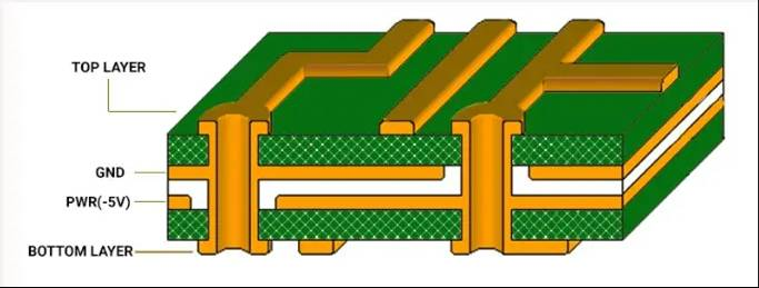
Via holes are used exclusively to establish electrical connections between PCB layers without mounting components. They are filled or plated with conductive material to allow signal and power transmission between different layers.
2. What are Types of Via Holes?
Through-Vias: Extend through all layers of a PCB, providing connections from the top to the bottom layer.
Blind Vias: Connect an outer layer to an internal layer but do not pass through the entire PCB thickness.
Buried Vias: Connect only internal layers and are not visible on the outer surfaces of the PCB.
Microvias: Extremely small vias used in high-density interconnect (HDI) PCBs, typically created using laser drilling.
3. What are the advantages of Via Technology?
Space Optimization: Enables complex multilayer designs with high component density.
Reduced Signal Interference: Proper via placement improves signal integrity in high-speed circuits.
Enhanced Thermal Management: Thermal vias help dissipate heat from high-power components.
4. What are the challenges of Via Technology?
Manufacturing Complexity: Laser-drilled microvias and buried vias require advanced fabrication processes.
Higher Cost: Additional processing steps increase PCB manufacturing costs.
Reliability Concerns: Poor via design can lead to signal loss or reliability issues under thermal cycling conditions.
Comparison of Through-Hole and Via Hole Technology
| Feature | Through-Hole Technology (THT) | Via Hole Technology |
| Purpose | Mechanical & electrical connections for component mounting | Electrical interconnections between PCB layers |
| Strength | High mechanical reliability | Suitable for high-density designs |
| Manufacturing Process | Drilled, component inserted, soldered | Drilled, plated, and filled with conductive material |
| Size | Larger hole size | Can be very small (especially microvias) |
| Application | Aerospace, automotive, power electronics | HDI PCBs, high-frequency circuits, compact devices |
What are the future trends of through-hole and via technology?
1. Advancements in Microvia Technology
As HDI PCBs become more common, microvia technology continues to evolve with improved laser drilling techniques and stacked microvias for enhanced electrical performance.
2. Hybrid Integration of THT and SMT
Modern PCB designs often combine THT and SMT to balance mechanical strength and space efficiency. Components requiring durability use through-holes, while high-density circuits rely on via technology.
3. Improved Reliability Testing
Enhanced via reliability testing methods, including thermal stress analysis and X-ray inspection, are being developed to prevent failure in high-speed and high-power applications.
Conclusion
Both through-hole and via hole technologies play essential roles in PCB design and manufacturing. Through-hole technology offers superior mechanical strength and reliability, making it suitable for high-power and rugged applications. Meanwhile, via hole technology is indispensable for modern high-density and high-speed circuit designs. By understanding their functions, advantages, and challenges, PCB designers can make informed decisions to optimize performance and manufacturability in advanced electronic applications.
-600x400-c.png)